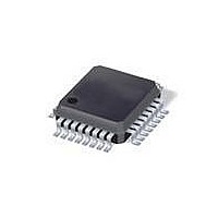
ATMEGA88PV-10AU Atmel, ATMEGA88PV-10AU Datasheet - Page 306

ATMEGA88PV-10AU
Manufacturer Part Number
ATMEGA88PV-10AU
Description
MCU AVR 8K ISP FLSH 10MHZ 32TQFP
Manufacturer
Atmel
Series
AVR® ATmegar
Specifications of ATMEGA88PV-10AU
Core Processor
AVR
Core Size
8-Bit
Speed
10MHz
Connectivity
I²C, SPI, UART/USART
Peripherals
Brown-out Detect/Reset, POR, PWM, WDT
Number Of I /o
23
Program Memory Size
8KB (4K x 16)
Program Memory Type
FLASH
Eeprom Size
512 x 8
Ram Size
1K x 8
Voltage - Supply (vcc/vdd)
1.8 V ~ 5.5 V
Data Converters
A/D 8x10b
Oscillator Type
Internal
Operating Temperature
-40°C ~ 85°C
Package / Case
32-TQFP, 32-VQFP
Processor Series
ATMEGA8x
Core
AVR8
Data Bus Width
8 bit
Data Ram Size
1 KB
Interface Type
SPI, TWI, UART
Maximum Clock Frequency
10 MHz
Number Of Programmable I/os
23
Number Of Timers
3
Operating Supply Voltage
1.8 V to 5.5 V
Maximum Operating Temperature
+ 85 C
Mounting Style
SMD/SMT
Minimum Operating Temperature
- 40 C
On-chip Adc
10 bit, 8 Channel
Package
32TQFP
Device Core
AVR
Family Name
ATmega
Maximum Speed
10 MHz
Controller Family/series
AVR MEGA
No. Of I/o's
23
Eeprom Memory Size
512Byte
Ram Memory Size
1KB
Cpu Speed
10MHz
Rohs Compliant
Yes
For Use With
ATAVRDRAGON - KIT DRAGON 32KB FLASH MEM AVRATAVRISP2 - PROGRAMMER AVR IN SYSTEM
Lead Free Status / RoHS Status
Lead free / RoHS Compliant
Available stocks
Company
Part Number
Manufacturer
Quantity
Price
- Current page: 306 of 420
- Download datasheet (9Mb)
27.8.3
Table 27-17. Serial Programming Instruction Set (Hexadecimal values)
8025L–AVR–7/10
Instruction/Operation
Programming Enable
Chip Erase (Program Memory/EEPROM)
Poll RDY/BSY
Load Instructions
Load Extended Address byte
Load Program Memory Page, High byte
Load Program Memory Page, Low byte
Load EEPROM Memory Page (page access)
Read Instructions
Read Program Memory, High byte
Read Program Memory, Low byte
Read EEPROM Memory
Read Lock bits
Read Signature Byte
Read Fuse bits
Read Fuse High bits
Read Extended Fuse Bits
Read Calibration Byte
Serial Programming Instruction set
6. Any memory location can be verified by using the Read instruction which returns the con-
7. At the end of the programming session, RESET can be set high to commence normal
8. Power-off sequence (if needed):
Table 27-16. Typical Wait Delay Before Writing the Next Flash or EEPROM Location
Table 27-17 on page 306
(1)
Symbol
t
t
t
WD_FLASH
WD_EEPROM
WD_ERASE
not used, the used must wait at least t
27-16). In a chip erased device, no 0xFF in the data file(s) need to be programmed.
tent at the selected address at serial output MISO.
operation.
Set RESET to “1”.
Turn V
CC
power off.
Byte 1
$AC
$AC
$4D
$C1
$A0
$F0
$48
$40
$28
$20
$58
$30
$50
$58
$50
$38
and
Figure 27-8 on page 308
0000 00aa
WD_EEPROM
adr MSB
adr MSB
Byte 2
$53
$80
$00
$00
$00
$00
$00
$00
$00
$00
$08
$08
$00
Instruction Format
before issuing the next byte (See
ATmega48P/88P/168P
describes the Instruction set.
Extended adr
0000 000aa
0000 000aa
aaaa aaaa
Minimum Wait Delay
adr LSB
adr LSB
adr LSB
adr LSB
Byte 3
$00
$00
$00
$00
$00
$00
$00
$00
4.5 ms
3.6 ms
9.0 ms
high data byte out
low data byte out
high data byte in
low data byte in
data byte out
data byte out
data byte out
data byte out
data byte out
data byte out
data byte out
data byte out
data byte in
Byte4
$00
$00
$00
Table
306
Related parts for ATMEGA88PV-10AU
Image
Part Number
Description
Manufacturer
Datasheet
Request
R

Part Number:
Description:
Manufacturer:
Atmel Corporation
Datasheet:

Part Number:
Description:
MCU AVR 8K ISP FLSH 20MHZ 32TQFP
Manufacturer:
Atmel
Datasheet:

Part Number:
Description:
MCU AVR 8K ISP FLASH 20MHZ 32QFN
Manufacturer:
Atmel
Datasheet:

Part Number:
Description:
MCU AVR 8K ISP FLASH 20MHZ 28DIP
Manufacturer:
Atmel
Datasheet:

Part Number:
Description:
MCU AVR 8KB FLASH 20MHZ 32TQFP
Manufacturer:
Atmel
Datasheet:

Part Number:
Description:
MCU AVR 8KB FLASH 20MHZ 32QFN
Manufacturer:
Atmel
Datasheet:

Part Number:
Description:
Atmega88p 8-bit Microcontroller With 8k Bytes In-system Programmable Flash
Manufacturer:
ATMEL Corporation
Datasheet:

Part Number:
Description:
IC MCU AVR 8K 5V 20MHZ 32-TQFP
Manufacturer:
Atmel
Datasheet:

Part Number:
Description:
Manufacturer:
Atmel Corporation
Datasheet:

Part Number:
Description:
Manufacturer:
Atmel Corporation
Datasheet:

Part Number:
Description:
MCU AVR 8K FLASH 15MHZ 32-QFN
Manufacturer:
Atmel
Datasheet:

Part Number:
Description:
IC AVR MCU 8K 20MHZ 5V 32TQFP
Manufacturer:
Atmel
Datasheet:

Part Number:
Description:
IC AVR MCU 8K 20MHZ 5V 32-QFN
Manufacturer:
Atmel
Datasheet:


