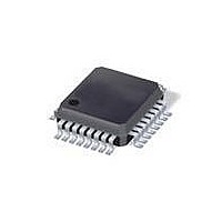
ATMEGA88PV-10AU Atmel, ATMEGA88PV-10AU Datasheet - Page 176

ATMEGA88PV-10AU
Manufacturer Part Number
ATMEGA88PV-10AU
Description
MCU AVR 8K ISP FLSH 10MHZ 32TQFP
Manufacturer
Atmel
Series
AVR® ATmegar
Specifications of ATMEGA88PV-10AU
Core Processor
AVR
Core Size
8-Bit
Speed
10MHz
Connectivity
I²C, SPI, UART/USART
Peripherals
Brown-out Detect/Reset, POR, PWM, WDT
Number Of I /o
23
Program Memory Size
8KB (4K x 16)
Program Memory Type
FLASH
Eeprom Size
512 x 8
Ram Size
1K x 8
Voltage - Supply (vcc/vdd)
1.8 V ~ 5.5 V
Data Converters
A/D 8x10b
Oscillator Type
Internal
Operating Temperature
-40°C ~ 85°C
Package / Case
32-TQFP, 32-VQFP
Processor Series
ATMEGA8x
Core
AVR8
Data Bus Width
8 bit
Data Ram Size
1 KB
Interface Type
SPI, TWI, UART
Maximum Clock Frequency
10 MHz
Number Of Programmable I/os
23
Number Of Timers
3
Operating Supply Voltage
1.8 V to 5.5 V
Maximum Operating Temperature
+ 85 C
Mounting Style
SMD/SMT
Minimum Operating Temperature
- 40 C
On-chip Adc
10 bit, 8 Channel
Package
32TQFP
Device Core
AVR
Family Name
ATmega
Maximum Speed
10 MHz
Controller Family/series
AVR MEGA
No. Of I/o's
23
Eeprom Memory Size
512Byte
Ram Memory Size
1KB
Cpu Speed
10MHz
Rohs Compliant
Yes
For Use With
ATAVRDRAGON - KIT DRAGON 32KB FLASH MEM AVRATAVRISP2 - PROGRAMMER AVR IN SYSTEM
Lead Free Status / RoHS Status
Lead free / RoHS Compliant
Available stocks
Company
Part Number
Manufacturer
Quantity
Price
- Current page: 176 of 420
- Download datasheet (9Mb)
19.3.1
8025L–AVR–7/10
Internal Clock Generation – The Baud Rate Generator
Figure 19-2
Figure 19-2. Clock Generation Logic, Block Diagram
Signal description:
operation.
Internal clock generation is used for the asynchronous and the synchronous master modes of
operation. The description in this section refers to
The USART Baud Rate Register (UBRRn) and the down-counter connected to it function as a
programmable prescaler or baud rate generator. The down-counter, running at system clock
(f
the UBRRnL Register is written. A clock is generated each time the counter reaches zero. This
clock is the baud rate generator clock output (= f
baud rate generator clock output by 2, 8 or 16 depending on mode. The baud rate generator out-
put is used directly by the Receiver’s clock and data recovery units. However, the recovery units
use a state machine that uses 2, 8 or 16 states depending on mode set by the state of the
UMSELn, U2Xn and DDR_XCKn bits.
osc
), is loaded with the UBRRn value each time the counter has counted down to zero or when
txclk
rxclk
xcki
xcko
fosc
DDR_XCKn
XCKn
Pin
shows a block diagram of the clock generation logic.
xcko
xcki
OSC
Transmitter clock (Internal Signal).
Receiver base clock (Internal Signal).
Input from XCK pin (internal Signal). Used for synchronous slave
Clock output to XCK pin (Internal Signal). Used for synchronous master
operation.
XTAL pin frequency (System Clock).
Down-Counter
Prescaling
Register
UBRRn
Sync
UBRRn+1
foscn
Detector
UCPOLn
Edge
/2
Figure
osc
/(UBRRn+1)). The Transmitter divides the
ATmega48P/88P/168P
/4
19-2.
/2
DDR_XCKn
U2Xn
0
1
0
1
0
1
1
0
UMSELn
txclk
rxclk
176
Related parts for ATMEGA88PV-10AU
Image
Part Number
Description
Manufacturer
Datasheet
Request
R

Part Number:
Description:
Manufacturer:
Atmel Corporation
Datasheet:

Part Number:
Description:
MCU AVR 8K ISP FLSH 20MHZ 32TQFP
Manufacturer:
Atmel
Datasheet:

Part Number:
Description:
MCU AVR 8K ISP FLASH 20MHZ 32QFN
Manufacturer:
Atmel
Datasheet:

Part Number:
Description:
MCU AVR 8K ISP FLASH 20MHZ 28DIP
Manufacturer:
Atmel
Datasheet:

Part Number:
Description:
MCU AVR 8KB FLASH 20MHZ 32TQFP
Manufacturer:
Atmel
Datasheet:

Part Number:
Description:
MCU AVR 8KB FLASH 20MHZ 32QFN
Manufacturer:
Atmel
Datasheet:

Part Number:
Description:
Atmega88p 8-bit Microcontroller With 8k Bytes In-system Programmable Flash
Manufacturer:
ATMEL Corporation
Datasheet:

Part Number:
Description:
IC MCU AVR 8K 5V 20MHZ 32-TQFP
Manufacturer:
Atmel
Datasheet:

Part Number:
Description:
Manufacturer:
Atmel Corporation
Datasheet:

Part Number:
Description:
Manufacturer:
Atmel Corporation
Datasheet:

Part Number:
Description:
MCU AVR 8K FLASH 15MHZ 32-QFN
Manufacturer:
Atmel
Datasheet:

Part Number:
Description:
IC AVR MCU 8K 20MHZ 5V 32TQFP
Manufacturer:
Atmel
Datasheet:

Part Number:
Description:
IC AVR MCU 8K 20MHZ 5V 32-QFN
Manufacturer:
Atmel
Datasheet:


