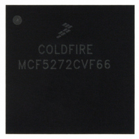
MCF5272CVF66 Freescale Semiconductor, MCF5272CVF66 Datasheet - Page 429

MCF5272CVF66
Manufacturer Part Number
MCF5272CVF66
Description
IC MPU 32BIT 66MHZ 196-MAPBGA
Manufacturer
Freescale Semiconductor
Series
MCF527xr
Specifications of MCF5272CVF66
Core Processor
Coldfire V2
Core Size
32-Bit
Speed
66MHz
Connectivity
EBI/EMI, Ethernet, I²C, SPI, UART/USART, USB
Peripherals
DMA, WDT
Number Of I /o
32
Program Memory Size
16KB (4K x 32)
Program Memory Type
ROM
Ram Size
1K x 32
Voltage - Supply (vcc/vdd)
3 V ~ 3.6 V
Oscillator Type
External
Operating Temperature
-40°C ~ 85°C
Package / Case
196-MAPBGA
Family Name
MCF5xxx
Device Core
ColdFire
Device Core Size
32b
Frequency (max)
66MHz
Instruction Set Architecture
RISC
Supply Voltage 1 (typ)
3.3V
Operating Temp Range
-40C to 85C
Operating Temperature Classification
Industrial
Mounting
Surface Mount
Pin Count
196
Package Type
MA-BGA
Lead Free Status / RoHS Status
Contains lead / RoHS non-compliant
Eeprom Size
-
Data Converters
-
Lead Free Status / Rohs Status
Not Compliant
Available stocks
Company
Part Number
Manufacturer
Quantity
Price
Company:
Part Number:
MCF5272CVF66
Manufacturer:
Freescale Semiconductor
Quantity:
10 000
Part Number:
MCF5272CVF66
Manufacturer:
FREESCALE
Quantity:
20 000
Company:
Part Number:
MCF5272CVF66 K75N
Manufacturer:
ST
Quantity:
18
Company:
Part Number:
MCF5272CVF66J
Manufacturer:
Freescale Semiconductor
Quantity:
10 000
- Current page: 429 of 544
- Download datasheet (7Mb)
19.3
The 23 dedicated address signals, A[22:0], define the address of external byte, word, and longword
accesses. These three-state outputs are the 23 lsbs of the internal 32-bit address bus and are multiplexed
with the SDRAM controller row and column addresses (SDA[13:0]).
Fourteen address signals are used for connecting to SDRAM devices as large as 256 Mbits.
The MCF5272 supports SDRAM widths of 16 or 32 bits. For a 32-bit width, SDRAM address signals are
multiplexed starting with A2. For a 16-bit width, address signals are multiplexed starting with A1.
19.4
The 32-bit, three-state, bidirectional, non-multiplexed data bus transfers data to and from the MCF5272.
A read or write operation can transfer 8, 16, or 32 bits in one bus cycle. When a 16-bit data bus is used,
mode parallel port C pins can be multiplexed onto D[15:0].
Data read from or written to on-chip peripherals is visible on the external data bus when the device’s
external bus width is 32 bits. When the device is configured for external 16-bit wide data bus and the data
access is 32 bits wide, the lower 16 bits of on-chip data are not visible externally. On-chip cache, ROM,
and SRAM accesses are not visible externally.
19.4.1
When the device is in normal mode, dynamic bus sizing lets the programmer change data bus width
between 8, 32, and 16 bits for each chip select. The initial width for the bootstrap program chip select, CS0,
is determined by the state of BUSW[1:0]. The program should select bus widths for the other chip selects
before accessing the associated memory space.
19.5
The eight chip selects, CS[7:0], allow the MCF5272 to interface directly to SRAM, EPROM, EEPROM,
and external memory-mapped peripherals. These signals can be programmed for an address location, with
masking capabilities, port size, burst capability indication, and wait-state generation.
CS0 provides a special function as a global chip select that allows access to boot ROM at reset. CS0 can
have its address redefined after reset. CS0 is the only chip select initialized and enabled during reset. All
other chip selects are disabled at reset and must be initialized by device initialization software.
CS7/SDCS can be configured to access RAM or ROM or one physical bank of SDRAM. Only CS7 can
be used for SDRAM chip select.
Freescale Semiconductor
Address Bus (A[22:0]/SDA[13:0])
Data Bus (D[31:0])
Chip Selects (CS7/SDCS, CS[6:0])
Dynamic Data Bus Sizing
MCF5272 ColdFire
®
Integrated Microprocessor User’s Manual, Rev. 3
Signal Descriptions
19-19
Related parts for MCF5272CVF66
Image
Part Number
Description
Manufacturer
Datasheet
Request
R
Part Number:
Description:
Mcf5272 Coldfire Integrated Microprocessor User
Manufacturer:
Freescale Semiconductor, Inc
Datasheet:

Part Number:
Description:
MCF5272 Interrupt Service Routine for the Physical Layer Interface Controller
Manufacturer:
Freescale Semiconductor / Motorola
Datasheet:
Part Number:
Description:
Manufacturer:
Freescale Semiconductor, Inc
Datasheet:
Part Number:
Description:
Manufacturer:
Freescale Semiconductor, Inc
Datasheet:
Part Number:
Description:
Manufacturer:
Freescale Semiconductor, Inc
Datasheet:
Part Number:
Description:
Manufacturer:
Freescale Semiconductor, Inc
Datasheet:
Part Number:
Description:
Manufacturer:
Freescale Semiconductor, Inc
Datasheet:
Part Number:
Description:
Manufacturer:
Freescale Semiconductor, Inc
Datasheet:
Part Number:
Description:
Manufacturer:
Freescale Semiconductor, Inc
Datasheet:
Part Number:
Description:
Manufacturer:
Freescale Semiconductor, Inc
Datasheet:
Part Number:
Description:
Manufacturer:
Freescale Semiconductor, Inc
Datasheet:
Part Number:
Description:
Manufacturer:
Freescale Semiconductor, Inc
Datasheet:
Part Number:
Description:
Manufacturer:
Freescale Semiconductor, Inc
Datasheet:
Part Number:
Description:
Manufacturer:
Freescale Semiconductor, Inc
Datasheet:
Part Number:
Description:
Manufacturer:
Freescale Semiconductor, Inc
Datasheet:


