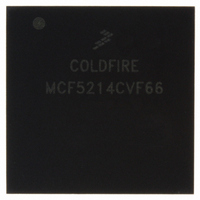
MCF5214CVF66 Freescale Semiconductor, MCF5214CVF66 Datasheet - Page 155

MCF5214CVF66
Manufacturer Part Number
MCF5214CVF66
Description
IC MPU 32BIT COLDF 256-MAPBGA
Manufacturer
Freescale Semiconductor
Series
MCF521xr
Datasheet
1.MCF5216CVM66J.pdf
(766 pages)
Specifications of MCF5214CVF66
Core Processor
Coldfire V2
Core Size
32-Bit
Speed
66MHz
Connectivity
CAN, EBI/EMI, I²C, SPI, UART/USART
Peripherals
DMA, LVD, POR, PWM, WDT
Number Of I /o
142
Program Memory Size
256KB (256K x 8)
Program Memory Type
FLASH
Ram Size
64K x 8
Voltage - Supply (vcc/vdd)
2.7 V ~ 3.6 V
Data Converters
A/D 8x12b
Oscillator Type
Internal
Operating Temperature
-40°C ~ 85°C
Package / Case
256-MAPBGA
Package
256MA-BGA
Device Core
ColdFire
Family Name
MCF521x
Maximum Speed
66 MHz
Operating Supply Voltage
3.3 V
Data Bus Width
32 Bit
Number Of Programmable I/os
142
Interface Type
QSPI/UART/I2C/CAN
On-chip Adc
8-chx10-bit
Number Of Timers
8
Lead Free Status / RoHS Status
Contains lead / RoHS non-compliant
Eeprom Size
-
Available stocks
Company
Part Number
Manufacturer
Quantity
Price
Company:
Part Number:
MCF5214CVF66
Manufacturer:
Freescale Semiconductor
Quantity:
10 000
Company:
Part Number:
MCF5214CVF66J
Manufacturer:
Freescale Semiconductor
Quantity:
10 000
- Current page: 155 of 766
- Download datasheet (9Mb)
See
8.4.2
The processor supports dual-ported local SRAM memory. This processor-local memory can be accessed
directly by the core and/or other system bus masters. Since this memory provides single-cycle accesses at
processor speed, it is ideal for applications where double-buffer schemes can be used to maximize
system-level performance. For example, a DMA channel in a typical double-buffer (also known as a
ping-pong scheme) application may load data into one portion of the dual-ported SRAM while the
processor is manipulating data in another portion of the SRAM. Once the processor completes the data
calculations, it begins processing the just-loaded buffer while the DMA moves out the just-calculated data
from the other buffer, and reloads the next data block into the just-freed memory region. The process
repeats with the processor and the DMA “ping-ponging” between alternate regions of the dual-ported
SRAM.
The processor design implements the dual-ported SRAM in the memory space defined by the RAMBAR
register. There are two physical copies of the RAMBAR register: one located in the processor core and
accessible only via the privileged MOVEC instruction at CPU space address 0xC05, and another located
in the SCM at IPSBAR + 0x008. ColdFire core accesses to this memory are controlled by the
processor-local copy of the RAMBAR, while module accesses are enabled by the SCM's RAMBAR.
Freescale Semiconductor
5. Chip Selects
Figure 8-1
31–30
Address
29–1
Bits
0
Reset
Reset
Field BA31 BA30
Field
R/W
R/W
Memory Base Address Register (RAMBAR)
Name
This is the list of memory access priorities when viewed from the processor
core.
31
15
and
0
BA
—
V
Table 8-2
30
1
Base address. Defines the base address of the 1-Gbyte internal peripheral space. This is the
starting address for the IPS registers when the valid bit is set.
Reserved, should be cleared.
Valid. Enables/disables the IPS Base address region. V is set at reset.
0 IPS Base address is not valid.
1 IPS Base address is valid.
MCF5282 and MCF5216 ColdFire Microcontroller User’s Manual, Rev. 3
29
Figure 8-1. IPS Base Address Register (IPSBAR)
for descriptions of the bits in IPSBAR.
Table 8-2. IPSBAR Field Description
NOTE
IPSBAR + 0x000
—
—
R/W
R/W
Description
—
—
System Control Module (SCM)
1
16
V
0
1
8-3
Related parts for MCF5214CVF66
Image
Part Number
Description
Manufacturer
Datasheet
Request
R
Part Number:
Description:
Manufacturer:
Freescale Semiconductor, Inc
Datasheet:
Part Number:
Description:
Manufacturer:
Freescale Semiconductor, Inc
Datasheet:
Part Number:
Description:
Manufacturer:
Freescale Semiconductor, Inc
Datasheet:
Part Number:
Description:
Manufacturer:
Freescale Semiconductor, Inc
Datasheet:
Part Number:
Description:
Manufacturer:
Freescale Semiconductor, Inc
Datasheet:
Part Number:
Description:
Manufacturer:
Freescale Semiconductor, Inc
Datasheet:
Part Number:
Description:
Manufacturer:
Freescale Semiconductor, Inc
Datasheet:
Part Number:
Description:
Manufacturer:
Freescale Semiconductor, Inc
Datasheet:
Part Number:
Description:
Manufacturer:
Freescale Semiconductor, Inc
Datasheet:
Part Number:
Description:
Manufacturer:
Freescale Semiconductor, Inc
Datasheet:
Part Number:
Description:
Manufacturer:
Freescale Semiconductor, Inc
Datasheet:
Part Number:
Description:
Manufacturer:
Freescale Semiconductor, Inc
Datasheet:
Part Number:
Description:
Manufacturer:
Freescale Semiconductor, Inc
Datasheet:
Part Number:
Description:
Manufacturer:
Freescale Semiconductor, Inc
Datasheet:
Part Number:
Description:
Manufacturer:
Freescale Semiconductor, Inc
Datasheet:


