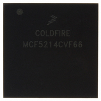
MCF5214CVF66 Freescale Semiconductor, MCF5214CVF66 Datasheet - Page 247

MCF5214CVF66
Manufacturer Part Number
MCF5214CVF66
Description
IC MPU 32BIT COLDF 256-MAPBGA
Manufacturer
Freescale Semiconductor
Series
MCF521xr
Datasheet
1.MCF5216CVM66J.pdf
(766 pages)
Specifications of MCF5214CVF66
Core Processor
Coldfire V2
Core Size
32-Bit
Speed
66MHz
Connectivity
CAN, EBI/EMI, I²C, SPI, UART/USART
Peripherals
DMA, LVD, POR, PWM, WDT
Number Of I /o
142
Program Memory Size
256KB (256K x 8)
Program Memory Type
FLASH
Ram Size
64K x 8
Voltage - Supply (vcc/vdd)
2.7 V ~ 3.6 V
Data Converters
A/D 8x12b
Oscillator Type
Internal
Operating Temperature
-40°C ~ 85°C
Package / Case
256-MAPBGA
Package
256MA-BGA
Device Core
ColdFire
Family Name
MCF521x
Maximum Speed
66 MHz
Operating Supply Voltage
3.3 V
Data Bus Width
32 Bit
Number Of Programmable I/os
142
Interface Type
QSPI/UART/I2C/CAN
On-chip Adc
8-chx10-bit
Number Of Timers
8
Lead Free Status / RoHS Status
Contains lead / RoHS non-compliant
Eeprom Size
-
Available stocks
Company
Part Number
Manufacturer
Quantity
Price
Company:
Part Number:
MCF5214CVF66
Manufacturer:
Freescale Semiconductor
Quantity:
10 000
Company:
Part Number:
MCF5214CVF66J
Manufacturer:
Freescale Semiconductor
Quantity:
10 000
- Current page: 247 of 766
- Download datasheet (9Mb)
Table 14-2
Freescale Semiconductor
Development serial
input/Test data
Development serial
output/Test data
Test clock
Debug data
Processor status
outputs
Test
QADC analog reference VRH, VRL
QADC analog supply
PLL analog supply
QADC positive supply
Flash erase/program
power
Flash array power
and ground
Standby power
Positive supply
Ground
lists signals in alphabetical order by abbreviated name.
Signal Name
MCF5282 and MCF5216 ColdFire Microcontroller User’s Manual, Rev. 3
Table 14-1. MCF5282 Signal Description (continued)
DSI/TDI
DSO/TDO
TCLK
DDATA[3:0]
PST[3:0]
TEST
VDDA, VSSA
VDDPLL, VSSPLL Isolate the PLL analog circuitry from
VDDH
VPP
VDDF, VSSF
VSTBY
VDD
VSS
Abbreviation
Power and Reference Signals
Provides single-bit communication for
debug module commands (DSI).
Provides serial data port for loading
JTAG boundary scan, bypass, and
instruction registers (TDI).
Provides single-bit communication for
debug module responses (DSO).
Provides serial data port for outputting
JTAG logic data (TDO).
JTAG test logic clock.
addresses, data, and breakpoint
status.
Indicate core status.
Reserved, should be connected to
VSS.
High (VRH) and low (VRL) reference
potentials for the analog converter.
digital power supply noise.
digital power supply noise.
Supplies positive power to the ESD
structures in the QADC pads.
Used for Flash stress testing.
Supply power and ground to Flash
array.
Provides standby voltage to RAM array
if VDD is lost.
Supplies positive power to the core
logic and I/O pads.
Negative supply.
Display captured processor
Test Signals
Isolate the QADC analog circuitry from
Function
Ground
I/O
O
O
O
I
I
I
I
I
I
I
I
I
I
Signal Descriptions
14-30
14-30
14-30
14-31
14-31
14-31
14-32
14-32
14-32
14-32
14-32
14-32
14-32
14-32
14-32
Page
14-7
Related parts for MCF5214CVF66
Image
Part Number
Description
Manufacturer
Datasheet
Request
R
Part Number:
Description:
Manufacturer:
Freescale Semiconductor, Inc
Datasheet:
Part Number:
Description:
Manufacturer:
Freescale Semiconductor, Inc
Datasheet:
Part Number:
Description:
Manufacturer:
Freescale Semiconductor, Inc
Datasheet:
Part Number:
Description:
Manufacturer:
Freescale Semiconductor, Inc
Datasheet:
Part Number:
Description:
Manufacturer:
Freescale Semiconductor, Inc
Datasheet:
Part Number:
Description:
Manufacturer:
Freescale Semiconductor, Inc
Datasheet:
Part Number:
Description:
Manufacturer:
Freescale Semiconductor, Inc
Datasheet:
Part Number:
Description:
Manufacturer:
Freescale Semiconductor, Inc
Datasheet:
Part Number:
Description:
Manufacturer:
Freescale Semiconductor, Inc
Datasheet:
Part Number:
Description:
Manufacturer:
Freescale Semiconductor, Inc
Datasheet:
Part Number:
Description:
Manufacturer:
Freescale Semiconductor, Inc
Datasheet:
Part Number:
Description:
Manufacturer:
Freescale Semiconductor, Inc
Datasheet:
Part Number:
Description:
Manufacturer:
Freescale Semiconductor, Inc
Datasheet:
Part Number:
Description:
Manufacturer:
Freescale Semiconductor, Inc
Datasheet:
Part Number:
Description:
Manufacturer:
Freescale Semiconductor, Inc
Datasheet:


