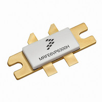
MRFE6VP6300HR5 Freescale Semiconductor, MRFE6VP6300HR5 Datasheet - Page 5

MRFE6VP6300HR5
Manufacturer Part Number
MRFE6VP6300HR5
Description
FET RF 2N-CH 230MHZ 125V NI780-4
Manufacturer
Freescale Semiconductor
Datasheet
1.MRFE6VP6300HR5.pdf
(14 pages)
Specifications of MRFE6VP6300HR5
Transistor Type
2 N-Channel (Dual)
Frequency
230MHz
Gain
26.5dB
Voltage - Rated
125V
Current - Test
100mA
Voltage - Test
50V
Power - Output
300W
Package / Case
NI-780H-4
Drain-source Breakdown Voltage
125 V
Gate-source Breakdown Voltage
10 V
Continuous Drain Current
100 mA
Maximum Operating Temperature
+ 150 C
Minimum Operating Temperature
- 65 C
Transistor Polarity
N-Channel
Lead Free Status / RoHS Status
Lead free / RoHS Compliant
Current Rating
-
Noise Figure
-
Other names
MRFE6VP6300HR5TR
Available stocks
Company
Part Number
Manufacturer
Quantity
Price
Company:
Part Number:
MRFE6VP6300HR5
Manufacturer:
FUJI
Quantity:
5 600
RF Device Data
Freescale Semiconductor
1000
90
80
70
60
50
40
30
20
100
29
28
27
26
25
24
23
22
0.1
10
20
Figure 4. Capacitance versus Drain- -Source Voltage
1
Figure 6. Pulsed Power Gain and Drain Efficiency
0
0
V
Pulse Width = 100 μsec, 20% Duty Cycle
G
η
DD
Note: Each side of device measured separately.
ps
D
Measured with ±30 mV(rms)ac @ 1 MHz
V
Figure 8. Pulsed Drain Efficiency versus
GS
= 50 Vdc, I
50
= 0 Vdc
V
DD
P
P
10
V
out
= 30 V
out
100
DS
DQ
, OUTPUT POWER (WATTS) PULSED
, OUTPUT POWER (WATTS) PULSED
, DRAIN--SOURCE VOLTAGE (VOLTS)
versus Output Power
= 100 mA, f = 230 MHz
V
Pulse Width = 100 μsec, 20% Duty Cycle
DD
150
Output Power
= 50 Vdc, I
20
35 V
100
200
DQ
= 100 mA, f = 230 MHz
250
30
TYPICAL CHARACTERISTICS — PULSED
40 V
300
45 V
40
350
C
50 V
C
C
oss
rss
iss
600
400
50
90
80
70
60
50
40
30
20
29
28
27
26
25
24
23
22
21
10
Figure 9. Pulsed Power Gain and Drain Efficiency
V
Pulse Width = 100 μsec, 20% Duty Cycle
60
59
58
57
56
55
54
53
T
29
28
27
26
25
24
23
22
21
20
19
DD
C
26
= --30_C
0
= 50 Vdc, I
V
Pulse Width = 100 μsec, 20% Duty Cycle
P1dB = 55.4 dBm
(344 W)
DD
85_C
P2dB = 55.8 dBm (380 W)
Figure 5. Pulsed Output Power versus
27
= 50 Vdc, I
η
50
P
Figure 7. Pulsed Power Gain versus
D
out
DQ
25_C
, OUTPUT POWER (WATTS) PULSED
P
versus Output Power
= 100 mA, f = 230 MHz
MRFE6VP6300HR3 MRFE6VP6300HSR3
out
P3dB = 56.0 dBm (398 W)
28
100
P
in
, OUTPUT POWER (WATTS) PULSED
DQ
, INPUT POWER (dBm) PULSED
V
G
= 100 mA, f = 230 MHz
DD
ps
150
= 30 V
V
Pulse Width = 100 μsec, 20% Duty Cycle
29
Output Power
Input Power
DD
= 50 Vdc, I
100
200
30
35 V
DQ
250
31
= 100 mA, f = 230 MHz
40 V
85_C
300
32
Actual
Ideal
45 V
25_C
--30_C
350
33
600
50 V
90
80
70
60
50
40
30
20
10
400
34
5


