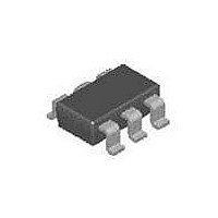
FDC658AP Fairchild Semiconductor, FDC658AP Datasheet - Page 2

FDC658AP
Manufacturer Part Number
FDC658AP
Description
MOSFET Small Signal -30VSgl P-Chl LogLv PwrTrch MOSFET
Manufacturer
Fairchild Semiconductor
Type
Power MOSFETr
Datasheet
1.FDC658AP.pdf
(5 pages)
Specifications of FDC658AP
Minimum Operating Temperature
- 55 C
Configuration
Single Quad Drain
Transistor Polarity
P-Channel
Resistance Drain-source Rds (on)
0.05 Ohm @ 10 V
Forward Transconductance Gfs (max / Min)
8.4 S
Drain-source Breakdown Voltage
30 V
Gate-source Breakdown Voltage
+/- 25 V
Continuous Drain Current
4 A
Power Dissipation
1600 mW
Maximum Operating Temperature
+ 150 C
Mounting Style
SMD/SMT
Package / Case
SuperSOT
Number Of Elements
1
Polarity
P
Channel Mode
Enhancement
Drain-source On-res
0.05Ohm
Drain-source On-volt
30V
Gate-source Voltage (max)
±25V
Output Power (max)
Not RequiredW
Frequency (max)
Not RequiredMHz
Noise Figure
Not RequireddB
Power Gain
Not RequireddB
Drain Efficiency
Not Required%
Operating Temp Range
-55C to 150C
Operating Temperature Classification
Military
Mounting
Surface Mount
Pin Count
6
Package Type
SuperSOT
Lead Free Status / RoHS Status
Lead free / RoHS Compliant
Available stocks
Company
Part Number
Manufacturer
Quantity
Price
Company:
Part Number:
FDC658AP
Manufacturer:
Fairchild Semiconductor
Quantity:
140 672
Part Number:
FDC658AP
Manufacturer:
FAIRCHILD/仙童
Quantity:
20 000
Part Number:
FDC658AP-NL
Manufacturer:
FAIRCHILD/仙童
Quantity:
20 000
FDC658AP Rev. B (W)
Electrical Characteristics
Off Characteristics
On Characteristics
Dynamic Characteristics
Switching Characteristics
Drain-Source Diode Characteristics and Maximum Ratings
Notes:
1: R
Scale 1: 1 on letter size paper
2: Pulse Test: Pulse Width < 300 µs, Duty Cycle < 2.0%
BV
∆BV
∆T
I
I
V
∆V
∆T
r
I
g
C
C
C
t
t
t
t
Q
Q
Q
I
V
DSS
GSS
DS(on)
D(ON)
d(on)
r
d(off)
f
S
FS
GS(TH)
SD
iss
oss
rss
g
gs
gd
the drain pins. R
Symbol
J
GS(TH)
J
DSS
θJA
DSS
is the sum of the junction-to-case and case-to-ambient thermal resistance where the case thermal reference is defined as the solder mounting surface of
Drain-Source Breakdown Voltage
Breakdown Voltage Temperature
Coefficient
Zero Gate Voltage Drain Current
Gate-Body Leakage
Gate Threshold Voltage
Gate Threshold Voltage
Temperature Coefficient
Static Drain-Source On-Resistance
On-State Drain Current
Forward Transconductance
Input Capacitance
Output Capacitance
Reverse Transfer Capacitance
Turn-On Delay Time
Turn-On Rise Time
Turn-Off Delay Time
Turn-Off Fall Time
Total Gate Charge
Gate-Source Charge
Gate-Drain Charge
Maximum Continuous Drain-Source Diode Forward Current
Drain-Source Diode Forward Voltage
θJC
is guaranteed by design while R
(Note 2)
Parameter
a) 78
1 in
o
C/W when mounted on a
2
pad of 2 oz copper
(Note 2)
T
θCA
J
= 25°C unless otherwise noted
is determined by the user's board design.
I
I
Referenced to 25°C
V
V
V
I
Referenced to 25°C
I
I
I
T
V
I
V
f = 1MHz
V
V
V
V
V
D
D
D
D
D
D
D
J
GS
GS
DS
GS
DS
DD
GS
DS
GS
GS
= -250µA, V
= -250µA,
= -250µA,
= -4A, V
= -3.4A, V
= -4A, V
= -4A, V
= 125°C
2
= V
= -15V, V
= -15V, I
= 0V, V
= ±25V, V
= -10V, V
= -15V, I
= -10V, R
= -5V
= 0V, I
Test Conditions
GS
, I
GS
GS
DS
S
DS
D
GS
= -1.3 A (Note 2)
D
D
= -5V
= -10V
= -10V,
GS
DS
GEN
GS
= -250µA
DS
= -4A,
= -24V
= -1A
= -4.5V
= -5V
= 0V,
= 0V
= 0V
= 6Ω
b) 156
minimum pad of 2 oz copper
o
Min
-30
C/W whe mounted on a
-20
-1
-0.77
Typ
-1.8
470
126
-22
8.4
2.1
61
44
67
60
12
16
4
7
6
6
2
www.fairchildsemi.com
±100
Max
-1.3
-1.2
8.1
-1
50
75
70
14
22
29
12
-3
mV/°C
mV/°C
Units
mΩ
µA
pF
pF
pF
nC
nC
nC
nA
ns
ns
ns
ns
V
V
A
S
A
V


