FXMA2102UMX Fairchild Semiconductor, FXMA2102UMX Datasheet
FXMA2102UMX
Specifications of FXMA2102UMX
Available stocks


Related parts for FXMA2102UMX


FXMA2102UMX Summary of contents
Page 1
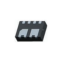
... HBM ESD (per JESD22-A114) - 2kV CDM (per JESD22-C101) Ordering Information Operating Part Number Temperature Range FXMA2102L8X -40 to +85°C FXMA2102UMX © 2010 Fairchild Semiconductor Corporation FXMA2102 • Rev. 1.0 Applications Description The FXMA2102 is a high-performance configurable dual-voltage-supply translator for bi-directional voltage translation over a wide range of input and output voltages levels ...
Page 2
... Block Diagram © 2010 Fairchild Semiconductor Corporation FXMA2102 • Rev. 1.0.2 Figure 1. Block Diagram Channels 2 www.fairchildsemi.com ...
Page 3
... CCB Truth Table Control OE LOW Logic Level HIGH Logic Level Note the OE pin is driven LOW, the FXMA2102 is disabled and the A drivers) are forced into 3-state. © 2010 Fairchild Semiconductor Corporation FXMA2102 • Rev. 1.0 GND Figure 3. UMLP (Top-Through View) A-Side Power Supply ...
Page 4
... CCB V Input Voltage IN Θ Thermal Resistance JA T Free Air Operating Temperature A Note: 3. All unused inputs and I/O pins must be held at V © 2010 Fairchild Semiconductor Corporation FXMA2102 • Rev. 1.0.2 Parameter A Port B Port Control Input (OE) A Outputs 3-State n B Outputs 3-State n A ...
Page 5
... The size of the pull-down resistor is based upon the current-sinking capability of the device driving the OE pin. Application Circuit © 2010 Fairchild Semiconductor Corporation FXMA2102 • Rev. 1.0.2 The recommended power-up sequence is Apply power to the first 0V, outputs are ...
Page 6
... FXMA2102 is attached to the master [on the A port] in this example, and there is a slave on the B port, the Npassgates act as a low resistive short between both © 2010 Fairchild Semiconductor Corporation FXMA2102 • Rev. 1.0.2 ports until either of the port’s V reached. After the RC time constant has reached the ...
Page 7
... This is well below PU the maximum edge rate of 300ns. Not only does the FXMA2102 drive 400pF, but it also provides excellent 2 headroom below the I C specification maximum edge rate of 300ns. © 2010 Fairchild Semiconductor Corporation FXMA2102 • Rev. 1.0 The I C specification mandates a maximum V ...
Page 8
... CC SCL Master SDA © 2010 Fairchild Semiconductor Corporation FXMA2102 • Rev. 1.0.2 condition from slave #2 to slave #1 as well as the master. However, if the OE pin is pulled LOW (disabled), both ports (A and B) are 3-stated. This results in the FXMA2102 isolating slave #2 from the master and slave #1, allowing full communication between the master and slave #1 ...
Page 9
... Care” indicates any valid logic level the V associated with the input side. CCI CC 8. Reflects current per supply, V © 2010 Fairchild Semiconductor Corporation FXMA2102 • Rev. 1.0.2 Conditions V CCA Data Inputs A 1.65–5.50 1.65–5. Control Input OE 1.65–5.50 1.65–5.50 0 Data Inputs B 1.65– ...
Page 10
... Direction CCA 4. 3. 2. 1.65V to 1.95V Notes: 13. F-toggle guaranteed by design simulation; not production tested. © 2010 Fairchild Semiconductor Corporation FXMA2102 • Rev. 1.0.2 = -40°C to +85°C. A 4.5 to 5.5V 3.0 to 3.6V Typ. Typ. (11 (12 -40°C to +85° CCB 4 ...
Page 11
... Skew is the variation of propagation delay between output signals and applies only to output signals on the same port ( and switching with the same polarity (LOW-to-HIGH or HIGH-to-LOW) (see Figure 15 Skew is guaranteed, but not tested. © 2010 Fairchild Semiconductor Corporation FXMA2102 • Rev. 1.0.2 = -40°C to +85° CCB 4.5 to 5.5V 3 ...
Page 12
... PHL t ( PZL ( PLZ n n Table 2. AC Load Table V CCO 1.8 ± 0.15V 2.5 ± 0.2V 3.3 ± 0.3V 5.0 ± 0.5V © 2010 Fairchild Semiconductor Corporation FXMA2102 • Rev. 1.0.2 Conditions GND CCA CCB , 5.0V GND 5. CCA CCB 5.0V CCA CCB IN Figure 8 ...
Page 13
... R F Input 2.0ns, 10 Input 2.5ns, 10 Input 2.5ns, 10 for control pin CCI CCA © 2010 Fairchild Semiconductor Corporation FXMA2102 • Rev. 1.0.2 V CCI V mi OUTPUT GND CONTROL t pxx V CCO V mo Figure 10. 3-STATE Output Low Enable Time (15 GND V x (15) ...
Page 14
... Package drawings are provided as a service to customers considering Fairchild components. Drawings may change in any manner without notice. Please note the revision and/or date on the drawing and contact a Fairchild Semiconductor representative to verify or obtain the most recent revision. Package specifications do not expand the terms of Fairchild’s worldwide terms and conditions, specifically the warranty therein, which covers Fairchild products. Always visit Fairchild Semiconductor’ ...
Page 15
... Package drawings are provided as a service to customers considering Fairchild components. Drawings may change in any manner without notice. Please note the revision and/or date on the drawing and contact a Fairchild Semiconductor representative to verify or obtain the most recent revision. Package specifications do not expand the terms of Fairchild’s worldwide terms and conditions, specifically the warranty therein, which covers Fairchild products. Always visit Fairchild Semiconductor’ ...
Page 16
... Fairchild Semiconductor Corporation FXMA2102 • Rev. 1.0.2 16 www.fairchildsemi.com ...