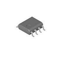
FL6961MY Fairchild Semiconductor, FL6961MY Datasheet

FL6961MY
Specifications of FL6961MY
Related parts for FL6961MY
FL6961MY Summary of contents
Page 1
... Construction and Ornamental LED Lighting Fixtures Ordering Information Operating Temperature Part Number Range FL6961MY -40°C to +125°C © 2010 Fairchild Semiconductor Corporation FL6961 • Rev. 1.0.1 Description The FL6961 is general lighting power controller for low to high power lumens applications requiring power factor correction ...
Page 2
... Figure 2. Block Diagram 2.65V 2.3V 1 INV 2.5V VOLTAGE REGULATOR UVLO V = 12V CC_ON V = 9.5V CC_OFF GND 6 © 2010 Fairchild Semiconductor Corporation FL6961 • Rev. 1.0 VCC INV 7 GATE COMP GND MOT ZCD Typical Application Circuit for Step-up Converter Typical Application Circuit for Single Stage PFC Converter ...
Page 3
... Driver Output. Totem-pole driver output to drive the external power MOSFET. The clamped gate 7 GATE output voltage is 16.5V Power Supply. Driver and control circuit supply voltage. CC © 2010 Fairchild Semiconductor Corporation FL6961 • Rev. 1.0.1 F- Fairchild Logo Z- Plant Code X- Year Code Y- Week Code TT: Die Run Code T: Package Type (M=SOP) ...
Page 4
... The Recommended Operating Conditions table defines the conditions for actual device operation. Recommended operating conditions are specified to ensure optimal performance to the datasheet specifications. Fairchild does not recommend exceeding them or designing to Absolute Maximum Ratings. Symbol T Operating Ambient Temperature A © 2010 Fairchild Semiconductor Corporation FL6961 • Rev. 1.0.1 Parameter Parameter 4 Min. Max. ...
Page 5
... Output Voltage Maximum (Clamp) Z OUT V Output Voltage Low OL V Output Voltage High OH t Rising Time R t Falling Time F © 2010 Fairchild Semiconductor Corporation FL6961 • Rev. 1.0.1 =-40°C to 125°C. Current is defined as positive into the device and J Conditions V =V – 0.16V CC CC-ON V =12V, V =0V ...
Page 6
... Disable Function Debounce Time ZCD-DIS Maximum On Time Section V Maximum On Time Voltage MOT Maximum On Time Programming t ON-MAX (Resistor Based) © 2010 Fairchild Semiconductor Corporation FL6961 • Rev. 1.0.1 =-40°C to 125°C. Current is defined as positive into the device and negative J Conditions V Increasing ZCD V Decreasing ...
Page 7
... Temperature (℃) Figure 8. t ON-MAX 10.5 10.1 9.7 9.3 8.9 8.5 -40 -25 - Temperature (℃) Figure 10. V th-OFF © 2010 Fairchild Semiconductor Corporation FL6961 • Rev. 1.0.1 3.0 2.4 1.8 1.2 0.6 0 110 125 -40 -25 -10 vs 14.0 13.4 12.8 12.2 11.6 11 ...
Page 8
... Temperature (℃) Figure 12. V MOT 0.87 0.85 0.83 0.81 0.79 0.77 -40 -25 - Temperature (℃) Figure 14 © 2010 Fairchild Semiconductor Corporation FL6961 • Rev. 1.0.1 (Continued) 18.0 17.4 16.8 16.2 15.6 15 110 125 vs 110 125 vs -40 -25 -10 5 ...
Page 9
... A high voltage in CS pin terminates a switching cycle immediately and cycle-by-cycle current limit is achieved. The designed threshold of the protection point is 0.82V. © 2010 Fairchild Semiconductor Corporation FL6961 • Rev. 1.0.1 Leading-Edge Blanking (LEB) A turn-on spike on CS pin appears when the power MOSFET is switched on ...
Page 10
... Package drawings are provided as a service to customers considering Fairchild components. Drawings may change in any manner without notice. Please note the revision and/or date on the drawing and contact a Fairchild Semiconductor representative to verify or obtain the most recent revision. Package specifications do not expand the terms of Fairchild’s worldwide terms and conditions, specifically the warranty therein, which covers Fairchild products. Always visit Fairchild Semiconductor’ ...
Page 11
... Fairchild Semiconductor Corporation FL6961 • Rev. 1.0.1 11 www.fairchildsemi.com ...


