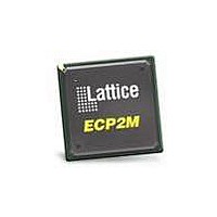
LFE2-12E-5TN144C Lattice, LFE2-12E-5TN144C Datasheet - Page 23

LFE2-12E-5TN144C
Manufacturer Part Number
LFE2-12E-5TN144C
Description
FPGA - Field Programmable Gate Array 12K LUTs 93 I/O DSP 1.2V -5 Spd
Manufacturer
Lattice
Datasheet
1.LFE2-12SE-6FN256C.pdf
(389 pages)
Specifications of LFE2-12E-5TN144C
Number Of Macrocells
12000
Number Of Programmable I/os
93
Data Ram Size
226304
Supply Voltage (max)
1.26 V
Maximum Operating Temperature
+ 85 C
Minimum Operating Temperature
0 C
Mounting Style
SMD/SMT
Supply Voltage (min)
1.14 V
Package / Case
TQFP-144
Lead Free Status / RoHS Status
Lead free / RoHS Compliant
Available stocks
Company
Part Number
Manufacturer
Quantity
Price
Company:
Part Number:
LFE2-12E-5TN144C
Manufacturer:
Lattice Semiconductor Corporation
Quantity:
10 000
- Current page: 23 of 389
- Download datasheet (5Mb)
Lattice Semiconductor
2. Write Through – A copy of the input data appears at the output of the same port during a write cycle. This
Memory Core Reset
The memory array in the EBR utilizes latches at the A and B output ports. These latches can be reset asynchro-
nously or synchronously. RSTA and RSTB are local signals, which reset the output latches associated with Port A
and Port B, respectively. The Global Reset (GSRN) signal resets both ports. The output data latches and associ-
ated resets for both ports are as shown in Figure 2-20.
Figure 2-20. Memory Core Reset
For further information about the sysMEM EBR block, please see the the list of additional technical documentation
at the end of this data sheet.
EBR Asynchronous Reset
EBR asynchronous reset or GSR (if used) can only be applied if all clock enables are low for a clock cycle before the
reset is applied and released a clock cycle after the reset is released, as shown in Figure 2-21. The GSR input to the
EBR is always asynchronous.
Figure 2-21. EBR Asynchronous Reset (Including GSR) Timing Diagram
If all clock enables remain enabled, the EBR asynchronous reset or GSR may only be applied and released after
the EBR read and write clock inputs are in a steady state condition for a minimum of 1/f
release must adhere to the EBR synchronous reset setup time before the next active read or write clock edge.
mode is supported for all data widths.
GSRN
RSTA
RSTB
Programmable Disable
Reset
Clock
Clock
Enable
Memory Core
2-20
Output Data
L
L
D
D
Latches
CLR
CLR
SET
SET
Q
Q
LatticeECP2/M Family Data Sheet
Port A[17:0]
Port B[17:0]
MAX
(EBR clock). The reset
Architecture
Related parts for LFE2-12E-5TN144C
Image
Part Number
Description
Manufacturer
Datasheet
Request
R

Part Number:
Description:
FPGA - Field Programmable Gate Array 12K LUTs 193 I/O DSP 1.2V -5 Spd
Manufacturer:
Lattice
Datasheet:

Part Number:
Description:
FPGA - Field Programmable Gate Array 12K LUTs 93 I/O DSP 1.2V -5 Spd I
Manufacturer:
Lattice

Part Number:
Description:
FPGA - Field Programmable Gate Array 12K LUTs 131 I/O DSP 1.2V -5 Spd
Manufacturer:
Lattice

Part Number:
Description:
FPGA - Field Programmable Gate Array 12K LUTs 93 I/O DSP 1.2V -5 Spd
Manufacturer:
Lattice

Part Number:
Description:
FPGA - Field Programmable Gate Array 12K LUTs 131 I/O DSP 1.2V -5 Spd I
Manufacturer:
Lattice

Part Number:
Description:
FPGA - Field Programmable Gate Array 12K LUTs 193 I/O DSP 1.2V -5 Spd I
Manufacturer:
Lattice
Part Number:
Description:
IC, LATTICEECP2 FPGA, 420MHZ, FPBGA-256
Manufacturer:
LATTICE SEMICONDUCTOR
Datasheet:

Part Number:
Description:
IC, LATTICEECP2 FPGA, 420MHZ, QFP-208
Manufacturer:
LATTICE SEMICONDUCTOR
Datasheet:

Part Number:
Description:
IC, LATTICEECP2 FPGA, 420MHZ, TQFP-144
Manufacturer:
LATTICE SEMICONDUCTOR
Datasheet:
Part Number:
Description:
FPGA LatticeECP2 Family 12000 Cells 90nm (CMOS) Technology 1.2V 256-Pin FBGA
Manufacturer:
LATTICE SEMICONDUCTOR
Datasheet:
Part Number:
Description:
FPGA LatticeECP2 Family 12000 Cells 90nm (CMOS) Technology 1.2V 256-Pin FBGA
Manufacturer:
LATTICE SEMICONDUCTOR
Datasheet:
Part Number:
Description:
FPGA LatticeECP2 Family 12000 Cells 90nm (CMOS) Technology 1.2V 484-Pin FBGA
Manufacturer:
LATTICE SEMICONDUCTOR
Datasheet:
Part Number:
Description:
FPGA LatticeECP2 Family 12000 Cells 90nm (CMOS) Technology 1.2V 256-Pin FBGA
Manufacturer:
LATTICE SEMICONDUCTOR
Datasheet:

Part Number:
Description:
FPGA LatticeECP2 Family 12000 Cells 90nm (CMOS) Technology 1.2V 208-Pin PQFP
Manufacturer:
Lattice
Datasheet:

Part Number:
Description:
IC FPGA 12KLUTS 131I/O 208-BGA
Manufacturer:
Lattice
Datasheet:


