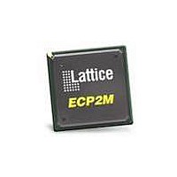
LFE2-12E-5TN144C Lattice, LFE2-12E-5TN144C Datasheet - Page 51

LFE2-12E-5TN144C
Manufacturer Part Number
LFE2-12E-5TN144C
Description
FPGA - Field Programmable Gate Array 12K LUTs 93 I/O DSP 1.2V -5 Spd
Manufacturer
Lattice
Datasheet
1.LFE2-12SE-6FN256C.pdf
(389 pages)
Specifications of LFE2-12E-5TN144C
Number Of Macrocells
12000
Number Of Programmable I/os
93
Data Ram Size
226304
Supply Voltage (max)
1.26 V
Maximum Operating Temperature
+ 85 C
Minimum Operating Temperature
0 C
Mounting Style
SMD/SMT
Supply Voltage (min)
1.14 V
Package / Case
TQFP-144
Lead Free Status / RoHS Status
Lead free / RoHS Compliant
Available stocks
Company
Part Number
Manufacturer
Quantity
Price
Company:
Part Number:
LFE2-12E-5TN144C
Manufacturer:
Lattice Semiconductor Corporation
Quantity:
10 000
- Current page: 51 of 389
- Download datasheet (5Mb)
Lattice Semiconductor
IEEE 1149.1-Compliant Boundary Scan Testability
All LatticeECP2/M devices have boundary scan cells that are accessed through an IEEE 1149.1 compliant Test
Access Port (TAP). This allows functional testing of the circuit board, on which the device is mounted, through a
serial scan path that can access all critical logic nodes. Internal registers are linked internally, allowing test data to
be shifted in and loaded directly onto test nodes, or test data to be captured and shifted out for verification. The test
access port consists of dedicated I/Os: TDI, TDO, TCK and TMS. The test access port has its own supply voltage
V
For more details on boundary scan test, please see information regarding additional technical documentation at
the end of this data sheet.
Device Configuration
All LatticeECP2/M devices contain two ports that can be used for device configuration. The Test Access Port (TAP),
which supports bit-wide configuration, and the sysCONFIG port, support both byte-wide and serial configuration,
including the standard SPI Flash interface. The TAP supports both the IEEE Standard 1149.1 Boundary Scan
specification and the IEEE Standard 1532 In- System Configuration specification. The sysCONFIG port is a 20-pin
interface with six I/Os used as dedicated pins with the remainder used as dual-use pins. See TN1108,
LatticeECP2/M sysCONFIG Usage Guide
Os.
On power-up, the FPGA SRAM is ready to be configured using the selected sysCONFIG port. Once a configuration
port is selected, it will remain active throughout that configuration cycle. The IEEE 1149.1 port can be activated any
time after power-up by sending the appropriate command through the TAP port.
Enhanced Configuration Option
LatticeECP2/M devices have enhanced configuration features such as: decryption support, TransFR™ I/O and
dual boot image support.
1. Decryption Support
2. TransFR (Transparent Field Reconfiguration)
3. Dual Boot Image Support
For more information about device configuration, please see the list of additional technical documentation at the
end of this data sheet.
Soft Error Detect (SED) Support
LatticeECP2/M devices have dedicated logic to perform CRC checks. During configuration, the configuration data
bitstream can be checked with the CRC logic block. In addition, the LatticeECP2 device can also be programmed
CCJ
LatticeECP2/M devices provide on-chip, One Time Programmable (OTP) non-volatile key storage to support
decryption of a 128-bit AES encrypted bitstream, securing designs and deterring design piracy.
TransFR I/O (TFR) is a unique Lattice technology that allows users to update their logic in the field without
interrupting system operation using a single ispVM
ing device configuration. This allows the device to be field updated with a minimum of system disruption and
downtime. See TN1087,
details.
Dual boot images are supported for applications requiring reliable remote updates of configuration data for the
system FPGA. After the system is running with a basic configuration, a new boot image can be downloaded
remotely and stored in a separate location in the configuration storage device. Any time after the update the
LatticeECP2/M can be re-booted from this new configuration file. If there is a problem, such as corrupt data
during download or incorrect version number with this new boot image, the LatticeECP2/M device can revert
back to the original backup configuration and try again. This all can be done without power cycling the system.
and can operate with LVCMOS3.3, 2.5, 1.8, 1.5 and 1.2 standards.
Minimizing System Interruption During Configuration Using TransFR
for more information about using the dual-use pins as general purpose I/
®
2-48
command. TransFR I/O allows I/O states to be frozen dur-
LatticeECP2/M Family Data Sheet
Technology, for
Architecture
Related parts for LFE2-12E-5TN144C
Image
Part Number
Description
Manufacturer
Datasheet
Request
R

Part Number:
Description:
FPGA - Field Programmable Gate Array 12K LUTs 193 I/O DSP 1.2V -5 Spd
Manufacturer:
Lattice
Datasheet:

Part Number:
Description:
FPGA - Field Programmable Gate Array 12K LUTs 93 I/O DSP 1.2V -5 Spd I
Manufacturer:
Lattice

Part Number:
Description:
FPGA - Field Programmable Gate Array 12K LUTs 131 I/O DSP 1.2V -5 Spd
Manufacturer:
Lattice

Part Number:
Description:
FPGA - Field Programmable Gate Array 12K LUTs 93 I/O DSP 1.2V -5 Spd
Manufacturer:
Lattice

Part Number:
Description:
FPGA - Field Programmable Gate Array 12K LUTs 131 I/O DSP 1.2V -5 Spd I
Manufacturer:
Lattice

Part Number:
Description:
FPGA - Field Programmable Gate Array 12K LUTs 193 I/O DSP 1.2V -5 Spd I
Manufacturer:
Lattice
Part Number:
Description:
IC, LATTICEECP2 FPGA, 420MHZ, FPBGA-256
Manufacturer:
LATTICE SEMICONDUCTOR
Datasheet:

Part Number:
Description:
IC, LATTICEECP2 FPGA, 420MHZ, QFP-208
Manufacturer:
LATTICE SEMICONDUCTOR
Datasheet:

Part Number:
Description:
IC, LATTICEECP2 FPGA, 420MHZ, TQFP-144
Manufacturer:
LATTICE SEMICONDUCTOR
Datasheet:
Part Number:
Description:
FPGA LatticeECP2 Family 12000 Cells 90nm (CMOS) Technology 1.2V 256-Pin FBGA
Manufacturer:
LATTICE SEMICONDUCTOR
Datasheet:
Part Number:
Description:
FPGA LatticeECP2 Family 12000 Cells 90nm (CMOS) Technology 1.2V 256-Pin FBGA
Manufacturer:
LATTICE SEMICONDUCTOR
Datasheet:
Part Number:
Description:
FPGA LatticeECP2 Family 12000 Cells 90nm (CMOS) Technology 1.2V 484-Pin FBGA
Manufacturer:
LATTICE SEMICONDUCTOR
Datasheet:
Part Number:
Description:
FPGA LatticeECP2 Family 12000 Cells 90nm (CMOS) Technology 1.2V 256-Pin FBGA
Manufacturer:
LATTICE SEMICONDUCTOR
Datasheet:

Part Number:
Description:
FPGA LatticeECP2 Family 12000 Cells 90nm (CMOS) Technology 1.2V 208-Pin PQFP
Manufacturer:
Lattice
Datasheet:

Part Number:
Description:
IC FPGA 12KLUTS 131I/O 208-BGA
Manufacturer:
Lattice
Datasheet:


