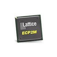
LFE2-12E-5TN144C Lattice, LFE2-12E-5TN144C Datasheet - Page 386

LFE2-12E-5TN144C
Manufacturer Part Number
LFE2-12E-5TN144C
Description
FPGA - Field Programmable Gate Array 12K LUTs 93 I/O DSP 1.2V -5 Spd
Manufacturer
Lattice
Datasheet
1.LFE2-12SE-6FN256C.pdf
(389 pages)
Specifications of LFE2-12E-5TN144C
Number Of Macrocells
12000
Number Of Programmable I/os
93
Data Ram Size
226304
Supply Voltage (max)
1.26 V
Maximum Operating Temperature
+ 85 C
Minimum Operating Temperature
0 C
Mounting Style
SMD/SMT
Supply Voltage (min)
1.14 V
Package / Case
TQFP-144
Lead Free Status / RoHS Status
Lead free / RoHS Compliant
Available stocks
Company
Part Number
Manufacturer
Quantity
Price
Company:
Part Number:
LFE2-12E-5TN144C
Manufacturer:
Lattice Semiconductor Corporation
Quantity:
10 000
- Current page: 386 of 389
- Download datasheet (5Mb)
www.latticesemi.com
© 2011 Lattice Semiconductor Corp. All Lattice trademarks, registered trademarks, patents, and disclaimers are as listed at www.latticesemi.com/legal. All other brand
or product names are trademarks or registered trademarks of their respective holders. The specifications and information herein are subject to change without notice.
April 2011
February 2006
August 2006
Date
Version
01.0
01.1
Pinout Information
DC and Switching
Characteristics
Introduction
Architecture
Section
—
LatticeECP2/M Family Data Sheet
Initial release.
Updated Table 1-1 “LatticeECP2 Family Selection Guide”.
Updated Figure 2-2 “PFU Diagram”.
Updated Figure 2-13 “Secondary Clock Regions ECP2-50”.
Updated Figure 2-25 “PIC Diagram”.
Updated Figure 2-26 “Input Register Block for Left, Right and Bottom
Edges”.
Updated Figure 2-28 “Output Register Block for Left, Right and Bottom
Edges”.
Updated Figure 2-30 “DQS Input Routing for Left and Right Edges”.
Updated Figure 2-32 “Edge Clock, DLL Calibration and DQS Local Bus
Distribution”.
Table 2-15 Selectable Master Clock (CCLK) Frequencies - Removed
frequencies 15, 20, 21, 22, 23, 30, 34, 41, 45, 51, 55, 60.
Replaced “CLKINDEL” with “CLKO”.
Updated SED section.
Qualified device migration capability when using DQS banks for DDR
interfaces.
Added VCCPLL to the Recommended Operating Conditions table.
Removed note 5 from “Hot Specifications” section.
Added notes 7 and 8 to “Initialization Supply” Current table.
Change note 6 - “...down to 95MHz” to “...down to 95MHz for DDR and
133MHz for DDR2” .
New “Typical Building Block Function Performance” numbers.
New External Switching Characteristics numbers.
New Internal Switching Characteristics numbers.
New Family Timing Adders numbers.
Updated Timings for GPLLs, SPLLs and DLLs.
Added sysCONFIG waveforms.
Remove HSTL15D_II from sysIO Recommended Operating Conditions
table.
Updated Supply and Initialization Currents for ECP2-50.
Added VCCPLL to the Signal Descriptions table.
Updated Logic Signal Connections tables to include 484-fpBGA for the
ECP2-50.
Added Logic Signal Connections tables for ECP2-12 devices.
Updated Pin Information Summary table to include ECP2-12.
Updated Power Supply and NC Connections table to include ECP2-12.
Added note 2 to DDR Strobe (DQS) Pin table.
Added Information on: PCI, DDR & SPI4.2 Capabilities of the device-
Package combination.
7-1
Change Summary
Revision History
DS1006 Revision History
Data Sheet DS1006
Related parts for LFE2-12E-5TN144C
Image
Part Number
Description
Manufacturer
Datasheet
Request
R

Part Number:
Description:
FPGA - Field Programmable Gate Array 12K LUTs 193 I/O DSP 1.2V -5 Spd
Manufacturer:
Lattice
Datasheet:

Part Number:
Description:
FPGA - Field Programmable Gate Array 12K LUTs 93 I/O DSP 1.2V -5 Spd I
Manufacturer:
Lattice

Part Number:
Description:
FPGA - Field Programmable Gate Array 12K LUTs 131 I/O DSP 1.2V -5 Spd
Manufacturer:
Lattice

Part Number:
Description:
FPGA - Field Programmable Gate Array 12K LUTs 93 I/O DSP 1.2V -5 Spd
Manufacturer:
Lattice

Part Number:
Description:
FPGA - Field Programmable Gate Array 12K LUTs 131 I/O DSP 1.2V -5 Spd I
Manufacturer:
Lattice

Part Number:
Description:
FPGA - Field Programmable Gate Array 12K LUTs 193 I/O DSP 1.2V -5 Spd I
Manufacturer:
Lattice
Part Number:
Description:
IC, LATTICEECP2 FPGA, 420MHZ, FPBGA-256
Manufacturer:
LATTICE SEMICONDUCTOR
Datasheet:

Part Number:
Description:
IC, LATTICEECP2 FPGA, 420MHZ, QFP-208
Manufacturer:
LATTICE SEMICONDUCTOR
Datasheet:

Part Number:
Description:
IC, LATTICEECP2 FPGA, 420MHZ, TQFP-144
Manufacturer:
LATTICE SEMICONDUCTOR
Datasheet:
Part Number:
Description:
FPGA LatticeECP2 Family 12000 Cells 90nm (CMOS) Technology 1.2V 256-Pin FBGA
Manufacturer:
LATTICE SEMICONDUCTOR
Datasheet:
Part Number:
Description:
FPGA LatticeECP2 Family 12000 Cells 90nm (CMOS) Technology 1.2V 256-Pin FBGA
Manufacturer:
LATTICE SEMICONDUCTOR
Datasheet:
Part Number:
Description:
FPGA LatticeECP2 Family 12000 Cells 90nm (CMOS) Technology 1.2V 484-Pin FBGA
Manufacturer:
LATTICE SEMICONDUCTOR
Datasheet:
Part Number:
Description:
FPGA LatticeECP2 Family 12000 Cells 90nm (CMOS) Technology 1.2V 256-Pin FBGA
Manufacturer:
LATTICE SEMICONDUCTOR
Datasheet:

Part Number:
Description:
FPGA LatticeECP2 Family 12000 Cells 90nm (CMOS) Technology 1.2V 208-Pin PQFP
Manufacturer:
Lattice
Datasheet:

Part Number:
Description:
IC FPGA 12KLUTS 131I/O 208-BGA
Manufacturer:
Lattice
Datasheet:


