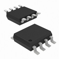
FAN73932MX Fairchild Semiconductor, FAN73932MX Datasheet

FAN73932MX
Specifications of FAN73932MX
Related parts for FAN73932MX
FAN73932MX Summary of contents
Page 1
... Motor Drive Inverter Ordering Information Part Number Package FAN73932M 8-SOP FAN73932MX For Fairchild’s definition of Eco Status, please visit: http://www.fairchildsemi.com/company/green/rohs_green.html. © 2008 Fairchild Semiconductor Corporation FAN73932 • Rev. 1.0.1 Description The FAN73932 is a half-bridge, gate-drive IC with shut- down and dead-time functions which can drive high- speed MOSFETs and IGBTs that operate up to +600V ...
Page 2
... Typical Application Diagrams +15V PWM PWM IC Shutdown Control Internal Block Diagram IN 1 SCHMITT TRIGGER INPUT 200K 5V SHOOT THOUGH PREVENTION 2 SD DEAD-TIME { 400ns } © 2008 Fairchild Semiconductor Corporation FAN73932 • Rev. 1.0 BOOT V COM BOOT Figure 1. Typical Application Circuit HS(ON/OFF) LS(ON/OFF) Figure 2. Functional Block Diagram ...
Page 3
... SD 3 COM © 2008 Fairchild Semiconductor Corporation FAN73932 • Rev. 1.0 COM Figure 3. Pin Configuration (Top View) Description Logic Input for High-Side and Low-Side Gate Driver Output, In-Phase with HO Logic Input for Shutdown Ground Low-Side Driver Return Supply Voltage High-Voltage Floating Supply Return ...
Page 4
... V Low-Side Output Voltage LO V Logic Input Voltage (IN Logic Input Voltage (SD Operating Ambient Temperature A Note: 4. Shutdown (SD) input is internally clamped with 5.2V. © 2008 Fairchild Semiconductor Corporation FAN73932 • Rev. 1.0.1 =25°C unless otherwise specified. A Parameter ( Parameter (4) Min. Max. Unit -0.3 625 -25 ...
Page 5
... Output High, Short-Circuit Pulsed Current O+ I Output Low, Short-Circuit Pulsed Current O- Allowable Negative Propagation to HO Note: 5 These parameters guaranteed by design. © 2008 Fairchild Semiconductor Corporation FAN73932 • Rev. 1.0.1 = 25°C, unless otherwise specified. The V A Test Condition V =0V, SD= =0V or 5V, SD= ...
Page 6
... R t Turn-Off Fall Time F Dead-Time: LO Turn-Off to HO Turn-On DT and HO Turn-Off to LO Turn-On MDT Dead-time matching=|DT Note: 6. The turn-on propagation delay time included dead-time. © 2008 Fairchild Semiconductor Corporation FAN73932 • Rev. 1.0.1 =1000pF, and T =25°C, unless otherwise specified Conditions ( ...
Page 7
... Temperature -40 - Temperature [°C] Figure 6. Turn-On Rise Time vs. Temperature -10 -20 -40 - Temperature [°C] Figure 8. Turn-On Delay Matching vs. Temperature © 2008 Fairchild Semiconductor Corporation FAN73932 • Rev. 1.0.1 280 240 200 160 120 100 120 -40 -20 Figure 5. Turn-Off Propagation Delay -10 -40 - 100 120 30 20 ...
Page 8
... Temperature [°C] Figure 12. Quiescent V DD vs. Temperature 1200 1000 800 600 400 200 -40 - Temperature [°C] Figure 14. Operating V DD vs. Temperature © 2008 Fairchild Semiconductor Corporation FAN73932 • Rev. 1.0.1 (Continued) 300 250 200 150 100 100 120 -40 Figure 11. Shutdown Propagation Delay 120 100 80 60 ...
Page 9
... Temperature [°C] Figure 20. High-Level Output Voltage vs. Temperature © 2008 Fairchild Semiconductor Corporation FAN73932 • Rev. 1.0.1 (Continued) 9.5 9.0 8.5 8.0 7.5 - 100 120 Figure 17. V 10.0 9.5 9.0 8.5 8.0 7 ...
Page 10
... Temperature [°C] Figure 22. Logic High Input Voltage vs. Temperature -40 - Temperature [°C] Figure 24. Logic Input High Bias Current vs. Temperature © 2008 Fairchild Semiconductor Corporation FAN73932 • Rev. 1.0.1 (Continued) 3.0 2.5 2.0 1.5 1.0 0 100 120 - -10 -11 -12 - 100 120 -40 Figure 25. Allowable Negative V ...
Page 11
... Switching Time Definitions SD LO 1nF DT1 DT2 IN 50 OFF R 90 © 2008 Fairchild Semiconductor Corporation FAN73932 • Rev. 1.0 COM Figure 26. Switching Time Test Circuit Shutdown DT1 DT2 DT2 Figure 27. Input/Output Timing Diagram 10 90% 10% Figure 28. Switching Time Waveform Definition +15V HO 10uF ...
Page 12
... 50% t OFF 90 IN(LO) 50% 50% IN(HO) 10% © 2008 Fairchild Semiconductor Corporation FAN73932 • Rev. 1.0.1 50 90% Figure 29. Shutdown Waveform Definition DT LO-HO 10% MDT LO-HO HO-LO Figure 30. Dead-Time Waveform Definition 10% Figure 31. Delay Matching Waveform Definition 50% DT HO-LO 10% 90% t OFF 50% 50% MT off 90% 90% www.fairchildsemi.com ...
Page 13
... Package drawings are provided as a service to customers considering Fairchild components. Drawings may change in any manner without notice. Please note the revision and/or date on the drawing and contact a Fairchild Semiconductor representative to verify or obtain the most recent revision. Package specifications do not expand the terms of Fairchild’s worldwide terms and conditions, specifically the warranty therein, which covers Fairchild products. Always visit Fairchild Semiconductor’ ...
Page 14
... Fairchild Semiconductor Corporation FAN73932 Rev. 1.0.1 14 www.fairchildsemi.com ...


