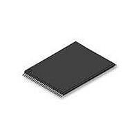
S29GL128P90TFIR10 Spansion Inc., S29GL128P90TFIR10 Datasheet - Page 12

S29GL128P90TFIR10
Manufacturer Part Number
S29GL128P90TFIR10
Description
IC, FLASH, 128MBIT, 90NS, TSOP-56
Manufacturer
Spansion Inc.
Datasheet
1.S29GL128P11TFI020.pdf
(80 pages)
Specifications of S29GL128P90TFIR10
Memory Type
Flash
Memory Size
128Mbit
Memory Configuration
16M X 8 / 8M X 16
Ic Interface Type
CFI, Parallel
Access Time
90ns
Supply Voltage Range
3.0 To 3.6 V
Memory Case Style
TSOP
Data Bus Width
8 bit, 16 bit
Architecture
Sectored
Interface Type
Serial
Supply Voltage (max)
3.6 V
Supply Voltage (min)
3 V
Maximum Operating Current
50 mA
Mounting Style
SMD/SMT
Operating Temperature
+ 85 C
Package / Case
TSOP-56
Lead Free Status / RoHS Status
Lead free / RoHS Compliant
Lead Free Status / RoHS Status
Lead free / RoHS Compliant, Lead free / RoHS Compliant
Available stocks
Company
Part Number
Manufacturer
Quantity
Price
Company:
Part Number:
S29GL128P90TFIR10
Manufacturer:
SPANSION
Quantity:
2 090
Part Number:
S29GL128P90TFIR10
Manufacturer:
SPANSION
Quantity:
20 000
Part Number:
S29GL128P90TFIR10D
Manufacturer:
SPANSION
Quantity:
20 000
3. Block Diagram
4. Physical Dimensions/Connection Diagrams
4.1
4.2
12
** A
A
Max
WP#/ACC
Max
RESET#
**–A0 (A-1)
BYTE#
GL01GP=A25, A
WE#
OE#
V
CE#
V
V
CC
SS
IO
Related Documents
Special Handling Instructions for BGA Package
This section shows the I/O designations and package specifications for the S29GL-P family.
The following documents contain information relating to the S29GL-P devices. Click on the title or go to
www.spansion.com
Special handling is required for Flash Memory products in BGA packages.
Flash memory devices in BGA packages may be damaged if exposed to ultrasonic cleaning methods. The
package and/or data integrity may be compromised if the package body is exposed to temperatures above
150°C for prolonged periods of time.
Max
RY/BY#
Considerations for X-ray Inspection of Surface-Mounted Flash Integrated Circuits
V
CC
Command
GL512P = A24, A
Register
Control
State
Detector
Max
download the PDF file, or request a copy from your sales office.
GL256P = A23, A
PGM Voltage
Generator
Figure 3.1 S29GL-P Block Diagram
Timer
S29GL-P MirrorBit
Max
Sector Switches
GL128P = A22
Erase Voltage
Generator
D a t a
STB
®
Flash Family
Output Enable
Chip Enable
S h e e t
Logic
Y-Decoder
X-Decoder
S29GL-P_00_A12 November 20, 2009
STB
DQ15
Input/Output
Buffers
Cell Matrix
Y-Gating
Latch
Data
–
DQ0


