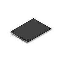
S29GL128P90TFIR10 Spansion Inc., S29GL128P90TFIR10 Datasheet - Page 40

S29GL128P90TFIR10
Manufacturer Part Number
S29GL128P90TFIR10
Description
IC, FLASH, 128MBIT, 90NS, TSOP-56
Manufacturer
Spansion Inc.
Datasheet
1.S29GL128P11TFI020.pdf
(80 pages)
Specifications of S29GL128P90TFIR10
Memory Type
Flash
Memory Size
128Mbit
Memory Configuration
16M X 8 / 8M X 16
Ic Interface Type
CFI, Parallel
Access Time
90ns
Supply Voltage Range
3.0 To 3.6 V
Memory Case Style
TSOP
Data Bus Width
8 bit, 16 bit
Architecture
Sectored
Interface Type
Serial
Supply Voltage (max)
3.6 V
Supply Voltage (min)
3 V
Maximum Operating Current
50 mA
Mounting Style
SMD/SMT
Operating Temperature
+ 85 C
Package / Case
TSOP-56
Lead Free Status / RoHS Status
Lead free / RoHS Compliant
Lead Free Status / RoHS Status
Lead free / RoHS Compliant, Lead free / RoHS Compliant
Available stocks
Company
Part Number
Manufacturer
Quantity
Price
Company:
Part Number:
S29GL128P90TFIR10
Manufacturer:
SPANSION
Quantity:
2 090
Part Number:
S29GL128P90TFIR10
Manufacturer:
SPANSION
Quantity:
20 000
Part Number:
S29GL128P90TFIR10D
Manufacturer:
SPANSION
Quantity:
20 000
7.9
40
7.9.1
7.9.2
Writing Commands/Command Sequences
RY/BY#
Hardware Reset
Notes
1. DQ5 switches to 1 when an Embedded Program, Embedded Erase, or Write-to-Buffer operation has exceeded the maximum timing limits.
2. DQ7 and DQ2 require a valid address when reading status information. Refer to the appropriate subsection for further details.
3. The Data# Polling algorithm should be used to monitor the last loaded write-buffer address location.
4. DQ1 switches to 1 when the device has aborted the write-to-buffer operation
During a write operation, the system must drive CE# and WE# to V
address, command, and data. Addresses are latched on the last falling edge of WE# or CE#, while data is
latched on the 1st rising edge of WE# or CE#. An erase operation can erase one sector, multiple sectors, or
the entire device.
address space is divided into uniform 64KW/128KB sectors. A sector address is the set of address bits
required to uniquely select a sector. I
the write mode. “AC Characteristics” contains timing specification tables and timing diagrams for write
operations.
The RY/BY# is a dedicated, open-drain output pin that indicates whether an Embedded Algorithm is in
progress or complete. The RY/BY# status is valid after the rising edge of the final WE# pulse in the command
sequence. Since RY/BY# is an open-drain output, several RY/BY# pins can be tied together in parallel with a
pull-up resistor to V
monitoring the RY/BY# pin, which is a dedicated output and controlled by CE# (not OE#).
The RESET# input provides a hardware method of resetting the device to reading array data. When RESET#
is driven low for at least a period of t
operation in progress, tristates all outputs, resets the configuration register, and ignores all read/write
commands for the duration of the RESET# pulse. The device also resets the internal state machine to reading
array data.
To ensure data integrity Program/Erase operations that were interrupted should be reinitiated once the device
is ready to accept another command sequence.
When RESET# is held at V
V
system to read the boot-up firmware from the Flash memory upon a system reset. See
on page 59
SS
Standard
Suspend
Suspend
Program
Write-to-
Refer
Erase
Buffer
Mode
Mode
Mode
, the standby current is greater. RESET# may be tied to the system reset circuitry which enables the
toDQ5: Exceeded Timing Limits on page 39
and
Program-
Suspend
Suspend
Embedded Program Algorithm
Erase-
Read
Read
Embedded Erase Algorithm
Erase-Suspend-Program
Figure 11.8 on page 60
(Embedded Program)
Table 6.1
Status
CC
Abort
Busy
. This feature allows the host system to detect when data is ready to be read by simply
Program-Suspended
Suspended Sector
Suspended Sector
Erase-Suspended
(Note 3)
(Note 4)
Non-Program
SS
Non-Erase
–
, the device draws V
S29GL-P MirrorBit
Sector
Sector
Table 6.4
RP
CC2
Table 7.17 Write Operation Status
(RESET# Pulse Width), the device immediately terminates any
indicate the address space that each sector occupies. The device
in “DC Characteristics” represents the active current specification for
for timing diagrams.
for more information.
(Note 2)
D a t a
DQ7#
DQ7#
DQ7#
DQ7#
DQ7
®
0
1
Flash Family
CC
reset current (I
No toggle
S h e e t
Toggle
Toggle
Toggle
Toggle
Toggle
DQ6
Invalid (not allowed)
(Note 1)
DQ5
IL
CC5
0
0
0
0
0
0
and OE# to V
Data
Data
). If RESET# is held at V
S29GL-P_00_A12 November 20, 2009
DQ3
N/A
N/A
N/A
N/A
N/A
1
No toggle
IH
(Note 2)
Toggle
Toggle
DQ2
when providing an
N/A
N/A
N/A
Figure 11.7
DQ1
N/A
N/A
N/A
IL
0
0
1
, but not at
BY#
RY/
0
0
1
1
1
1
0
0
0


