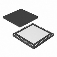
PIC24FJ256GB106-I/MR Microchip Technology, PIC24FJ256GB106-I/MR Datasheet - Page 268

PIC24FJ256GB106-I/MR
Manufacturer Part Number
PIC24FJ256GB106-I/MR
Description
IC, 16BIT MCU, PIC24F, 32MHZ, QFN-64
Manufacturer
Microchip Technology
Series
PIC® 24Fr
Datasheets
1.PIC24FJ128GA106-IPT.pdf
(52 pages)
2.PIC24FJ64GB106-IPT.pdf
(16 pages)
3.PIC24FJ64GB106-IPT.pdf
(352 pages)
4.PIC24FJ192GB108-IPT.pdf
(328 pages)
Specifications of PIC24FJ256GB106-I/MR
Controller Family/series
PIC24
No. Of I/o's
51
Ram Memory Size
16KB
Cpu Speed
32MHz
No. Of Timers
5
Core Size
16 Bit
Program Memory Size
256KB
Peripherals
ADC, Comparator, PWM, RTC, Timer
Core Processor
PIC
Speed
32MHz
Connectivity
I²C, SPI, UART/USART, USB OTG
Number Of I /o
51
Program Memory Type
FLASH
Ram Size
16K x 8
Voltage - Supply (vcc/vdd)
2 V ~ 3.6 V
Data Converters
A/D 16x10b
Oscillator Type
Internal
Operating Temperature
-40°C ~ 85°C
Package / Case
64-VFQFN, Exposed Pad
Processor Series
PIC24FJ
Core
PIC
Data Bus Width
16 bit
Data Ram Size
16 KB
Interface Type
I2C, SPI, UART
Maximum Clock Frequency
32 MHz
Number Of Programmable I/os
52
Number Of Timers
5
Maximum Operating Temperature
+ 85 C
Mounting Style
SMD/SMT
3rd Party Development Tools
52713-733, 52714-737, 53276-922, EWDSPIC
Development Tools By Supplier
PG164130, DV164035, DV244005, DV164005, PG164120, DM240001, DM240011
Minimum Operating Temperature
- 40 C
On-chip Adc
10 bit, 16 Channel
Lead Free Status / RoHS Status
Lead free / RoHS Compliant
For Use With
876-1004 - PIC24 BREAKOUT BOARD
Eeprom Size
-
Lead Free Status / Rohs Status
Details
Available stocks
Company
Part Number
Manufacturer
Quantity
Price
Company:
Part Number:
PIC24FJ256GB106-I/MR
Manufacturer:
TI
Quantity:
1 292
- PIC24FJ128GA106-IPT PDF datasheet
- PIC24FJ64GB106-IPT PDF datasheet #2
- PIC24FJ64GB106-IPT PDF datasheet #3
- PIC24FJ192GB108-IPT PDF datasheet #4
- Current page: 268 of 328
- Download datasheet (6Mb)
PIC24FJ256GB110 FAMILY
24.2
Time measurements on the pulse width can be similarly
performed, using the A/D module’s internal capacitor
(C
Figure 24-2 shows the external connections used for
time measurements, and how the CTMU and A/D mod-
ules are related in this application. This example also
shows both edge events coming from the external
CTEDG pins, but other configurations using internal
edge sources are possible. A detailed discussion on
measuring capacitance and time with the CTMU module
is provided in the PIC24F Family Reference Manual.
24.3
The CTMU module can also generate an output pulse
with edges that are not synchronous with the device’s
system clock. More specifically, it can generate a pulse
with a programmable delay from an edge event input to
the module.
FIGURE 24-2:
FIGURE 24-3:
DS39897B-page 266
AD
) and a precision resistor for current calibration.
Measuring Time
Pulse Generation and Delay
TYPICAL CONNECTIONS AND INTERNAL CONFIGURATION FOR TIME
MEASUREMENT TIME
TYPICAL CONNECTIONS AND INTERNAL CONFIGURATION FOR PULSE
DELAY GENERATION
CTEDG1
C2INB
C
CTEDG1
CTEDG2
DELAY
ANx
R
PR
EDG1
CV
EDG2
Preliminary
EDG1
Current Source
PIC24F Device
Comparator
REF
C
AD
PIC24F Device
A/D Converter
CTMU
C2
Current Source
CTMU
Output Pulse
When the module is configured for pulse generation
delay by setting the TGEN bit (CTMUCON<12>), the
internal current source is connected to the B input of
Comparator 2. A capacitor (C
the Comparator 2 pin, C2INB, and the comparator volt-
age reference, CV
is then configured for a specific trip point. The module
begins to charge C
detected. When C
point, a pulse is output on CTPLS. The length of the
pulse delay is determined by the value of C
the CV
Figure 24-3 shows the external connections for pulse
generation, as well as the relationship of the different
analog modules required. While CTEDG1 is shown as
the input pulse source, other options are available. A
detailed discussion on pulse generation with the CTMU
module is provided in the “PIC24F Family Reference
Manual”.
REF
trip point.
DELAY
REF
CTPLS
DELAY
, is connected to C2INA. CV
© 2008 Microchip Technology Inc.
charges above the CV
when an edge event is
DELAY
) is connected to
DELAY
REF
and
REF
trip
Related parts for PIC24FJ256GB106-I/MR
Image
Part Number
Description
Manufacturer
Datasheet
Request
R

Part Number:
Description:
Manufacturer:
Microchip Technology Inc.
Datasheet:

Part Number:
Description:
Manufacturer:
Microchip Technology Inc.
Datasheet:

Part Number:
Description:
Manufacturer:
Microchip Technology Inc.
Datasheet:

Part Number:
Description:
Manufacturer:
Microchip Technology Inc.
Datasheet:

Part Number:
Description:
Manufacturer:
Microchip Technology Inc.
Datasheet:

Part Number:
Description:
Manufacturer:
Microchip Technology Inc.
Datasheet:

Part Number:
Description:
Manufacturer:
Microchip Technology Inc.
Datasheet:

Part Number:
Description:
Manufacturer:
Microchip Technology Inc.
Datasheet:


