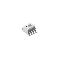
FOD060LR2 Fairchild Semiconductor, FOD060LR2 Datasheet

FOD060LR2
Specifications of FOD060LR2
Related parts for FOD060LR2
FOD060LR2 Summary of contents
Page 1
... NC* L* NC* *Dual channel devices or single channel devices with pin 7 not connected. A 0.1 µF bypass capacitor must be connected between pins 8 and 5. (See note 1) ©2008 Fairchild Semiconductor Corporation FOD060L, FOD260L, FOD063L Rev. 1.0.3 Data multiplexing Switching power supplies Pulse transformer replacement Computer-peripheral interface ...
Page 2
... Enable Voltage, High Level (Single Channel) Operating Temperature Fan Out (TTL load) Output Pull-up Resistor *6 guard banded value which allows for at least 20% CTR degradation. Initial input current threshold value is 5 less. ©2008 Fairchild Semiconductor Corporation FOD060L, FOD260L, FOD063L Rev. 1.0.3 (No derating required up to 85°C) Symbol T ...
Page 3
... Common Mode (R Transient Immunity ( mA (at Output High Level) Common Mode (R Transient Immunity (I = 7.5 mA (at Output Low Level) ©2008 Fairchild Semiconductor Corporation FOD060L, FOD260L, FOD063L Rev. 1.0 -40°C to +85°C unless otherwise specified.) A Test Conditions Symbol Min Typ** Max Unit ( MHz ...
Page 4
... L (i.e., V < 0.8 V). Measured in volts per microsecond (V/µs). OUT 12. Device considered a two-terminal device: Pins 1,2,3 and 4 shorted together, and Pins 5,6,7 and 8 shorted together. ©2008 Fairchild Semiconductor Corporation FOD060L, FOD260L, FOD063L Rev. 1.0 -40°C to +85°C Unless otherwise specified.) A Test Conditions Symbol (I = 250 µ ...
Page 5
... Ambient Temperature ( C) A Fig. 5 Low Level Output Current vs. Ambient Temperature 3. (Single channel products only 0. 5mA -40 - Ambient Temperature ( C) A ©2008 Fairchild Semiconductor Corporation FOD060L, FOD260L, FOD063L Rev. 1.0 - 1.4 1.5 1.6 1 100 60 80 100 5 Fig. 2 Input Threshold Current vs. Ambient Temperature 2 3. 0.6V O 2.0 FOD063L ...
Page 6
... Typical Performance Curves Fig. 7 Rise and Fall Times vs. Ambient Temperature 3. 7.5mA 350 -40 - Ambient Temperature ( C) A ©2008 Fairchild Semiconductor Corporation FOD060L, FOD260L, FOD063L Rev. 1.0 100 6 Fig. 8 Pulse Width Distortion vs. Ambient Temperature 7.5mA 350 FOD260L FOD060L FOD063L 5 0 -40 - Ambient Temperature ( C) A www.fairchildsemi.com ...
Page 7
... L Bypass Input Monitor GND 5 47 Test Circuit for FOD060L, and FOD260L Fig. 9 Test Circuit and Waveforms for t Pulse Generator tr = 5ns 7 ©2008 Fairchild Semiconductor Corporation FOD060L, FOD260L, FOD063L Rev. 1.0.3 Pulse Gen Dual Channel Input 2 7 Monitoring Node 0.1 F Output 3 6 Bypass ...
Page 8
... GND V CM Pulse Gen Test Circuit for FOD060L and FOD260L Peak 3. 0.5 V Fig. 11 Test Circuit Common Mode Transient Immunity ©2008 Fairchild Semiconductor Corporation FOD060L, FOD260L, FOD063L Rev. 1.0 +3. 0.1 f 350 bypass V FF Output Switching Pos. (A (Min (Max) O Switching Pos Dual Channel +3 ...
Page 9
... TYP Lead Coplanarity : 0.004 (0.10) MAX ©2008 Fairchild Semiconductor Corporation FOD060L, FOD260L, FOD063L Rev. 1.0.3 0.275 (6.99) 0.010 (0.25) 0.006 (0.16) 0.244 (6.19) 0.224 (5.69) 9 8-Pin Small Outline ...
Page 10
... TYP NOTE All dimensions are in inches (millimeters) ©2008 Fairchild Semiconductor Corporation FOD060L, FOD260L, FOD063L Rev. 1.0.3 Package Dimensions (Surface Mount) 0.390 (9.91) 0.370 (9.40 0.200 (5.08) 0.140 (3.55) 15° ...
Page 11
... FOD260L FOD060L S FOD260LS SD FOD260LSD SV Pending Approval SDV Pending Approval T FOD260LT TV Pending Approval R1 FOD060LR1 R1V Pending Approval R2 FOD060LR2 R2V Pending Approval V Pending Approval Marking Information DIP 260L Definitions 1 Fairchild logo 2 Device number 3 VDE mark (Note: Only appears on parts ordered with VDE option – ...
Page 12
... Peak reflow temperature • Time of temperature higher than 245 C • Number of reflows 300 250 200 150 100 50 ©2008 Fairchild Semiconductor Corporation FOD060L, FOD260L, FOD063L Rev. 1.0.3 12.0 ±0.1 4.0 ±0.1 4.0 ±0.1 10.30 ±0.20 User Direction of Feed 260 C (package surface temperature) 40 seconds or less ...
Page 13
... C 140 120 100 ©2008 Fairchild Semiconductor Corporation FOD060L, FOD260L, FOD063L Rev. 1.0.3 8.0 0.10 2.0 0.05 4.0 0.10 6.40 0.20 260 C Time above 183 Sec 1.822 C/Sec Ramp up rate 33 Sec 60 120 180 Time (s) 13 Ø ...
Page 14
... TRADEMARKS The following includes registered and unregistered trademarks and service marks, owned by Fairchild Semiconductor and/or its gl o bal subsidiaries, and is not intended exhaustive list of all such trademarks. AccuPower™ F-PFS™ FRFET Auto-SPM™ Build it Now™ Global Power Resource Green FPS™ ...


