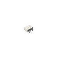
MOC3083SM Fairchild Semiconductor, MOC3083SM Datasheet - Page 2

MOC3083SM
Manufacturer Part Number
MOC3083SM
Description
Triac & SCR Output Optocouplers 6Pin800V Optocoupler Zero Cross Triac Dr
Manufacturer
Fairchild Semiconductor
Datasheet
1.MOC3083M.pdf
(11 pages)
Specifications of MOC3083SM
Configuration
1
Maximum Input Current
60 mA
Maximum Operating Temperature
+ 85 C
Maximum Power Dissipation
250 mW
Maximum Reverse Diode Voltage
6 V
Minimum Operating Temperature
- 40 C
Output Type
AC
Package / Case
PDIP SMD White
Typical Input Voltage
1.3 V
Zero-crossing Circuit
Yes
Zero-crossing Voltage
20 V
Output Device
PhotoTriac
Isolation Voltage
7.5 kV
Peak Output Voltage (vdrm)
800 V
Maximum Input Voltage
1.5 V
Maximum Output Voltage
560 VAC
Minimum Trigger Current
5 mA (Max)
Number Of Elements
1
Forward Voltage
1.5V
Repetitive Peak Off-state Volt
800V
Operating Temp Range
-40C to 85C
Package Type
PDIP W SMD
Reverse Breakdown Voltage
6V
Mounting
Surface Mount
Pin Count
6
Trigger Current
5mA
Zero Crossing Circuit
Yes
Operating Temperature Classification
Industrial
Forward Current
60mA
Power Dissipation
250mW
Lead Free Status / RoHS Status
Lead free / RoHS Compliant
Available stocks
Company
Part Number
Manufacturer
Quantity
Price
Company:
Part Number:
MOC3083SM
Manufacturer:
Fairchild Optoelectronics Grou
Quantity:
135
©2005 Fairchild Semiconductor Corporation
MOC3081M, MOC3082M, MOC3083M Rev. 1.0.3
Absolute Maximum Ratings
Stresses exceeding the absolute maximum ratings may damage the device. The device may not function or be
operable above the recommended operating conditions and stressing the parts to these levels is not recommended.
In addition, extended exposure to stresses above the recommended operating conditions may affect device reliability.
The absolute maximum ratings are stress ratings only.
Note:
1. Isolation surge voltage, V
TOTAL DEVICE
EMITTER
DETECTOR
common, and Pins 4, 5 and 6 are common.
Symbol
V
T
T
T
V
I
TSM
OPR
P
V
P
DRM
P
STG
T
SOL
I
ISO
F
D
R
D
D
J
Storage Temperature
Operating Temperature
Lead Solder Temperature
Junction Temperature Range
Isolation Surge Voltage
Total Device Power Dissipation @ 25°C Ambient
Continuous Forward Current
Reverse Voltage
Total Power Dissipation @ 25°C Ambient
Off-State Output Terminal Voltage
Peak Repetitive Surge Current (PW = 100µs, 120pps)
Total Power Dissipation @ 25°C Ambient
Derate above 25°C
Derate above 25°C
Derate above 25°C
ISO
, is an internal device dielectric breakdown rating. For this test, Pins 1 and 2 are
(1)
(T
A
(peak AC voltage, 60Hz, 1 sec. duration)
= 25°C unless otherwise noted)
Parameters
2
260 for 10 sec
-40 to +150
-40 to +100
-40 to +85
Value
7500
2.94
1.41
1.76
250
120
800
150
60
6
1
www.fairchildsemi.com
Vac(pk)
mW/°C
mW/°C
mW/°C
Units
mW
mW
mW
mA
°C
°C
°C
°C
V
V
A


