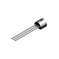
BF244C_Q Fairchild Semiconductor, BF244C_Q Datasheet - Page 3

BF244C_Q
Manufacturer Part Number
BF244C_Q
Description
RF JFET N-Ch RF amplifier
Manufacturer
Fairchild Semiconductor
Datasheet
1.BF244B_Q.pdf
(6 pages)
Specifications of BF244C_Q
Configuration
Single
Mounting Style
Through Hole
Minimum Operating Temperature
- 55 C
Transistor Polarity
N-Channel
Gate-source Breakdown Voltage
- 30 V
Maximum Drain Gate Voltage
30 V
Continuous Drain Current
50 mA
Power Dissipation
350 mW
Maximum Operating Temperature
+ 150 C
Package / Case
TO-92
Lead Free Status / RoHS Status
Lead free / RoHS Compliant
Typical Characteristics
0.5
0.1
7
6
5
4
3
2
1
0
20
10
0.5
0.1
10
5
1
0.01 0.02
0
5
1
0.01 0.02
T = +25 C
f = 1.0 kHz
V
A
GS(OFF)
-2.5 V
V
T = +125 C
Output Conductance vs
T
T = +25 C
V
-1
A
A
Transconductance vs
V - GATE-SOURCE VOLTAGE(V)
DG
A
G S(OFF)
O
0.05 0.1
T
= - 1.5V
0.05 0.1
GS
Transconductance
= -55 C
A
= 5v
10
I -- DRAIN CURRENT (mA)
I
20
D
D
Characteristics
= -55 C
Drain Current
T = +25 C
Drain Current
- DRAIN CURRENT (mA)
= -1.5V
A
O
O
O
15
O
-2
V
V
0.2
V
T = +125 C
0.2
G S(OFF)
A
GS(OFF)
G S(OFF)
O
10
15
5
20
0.5
0.5
= -5.5V
= -3.5V
= - 5V
-3
T
O
A
1
= -55 C
T = +25 C
1
V
A
V
(continued)
GS(OFF)
T = +25 C
T = +125 C
T = +125 C
T
DS
2
f = 1.0 kHz
2
A
A
O
V
A
A
-4
DG
= -55 C
= 15V
O
= 15V
= -4.5V
15V
5.0V
10V
5
20V
5
O
O
O
O
10
10
-5
20
10
5
4
3
2
1
0
-
1
10
0
gfs, I
5
1
0.01 0.03
T = +25 C
TYP V
A
V
BW = 6.0 Hz @ f = 10 Hz, 100 Hz
I = 3 mA
DG
DSS
D
V - GATE-SOURCE VOLTAGE(V)
Noise Voltage vs Frequency
Parameter Interactions
r
= 0.2 f @ f > 1.0 kHz
GS
DS
= 15V
GS(OFF)
Common Drain-Source
0.2
V
Transconductance
O
@ V
@ V = 100mV, V
DS
-
V
2
0.1
- DRAIN-SOURCE VOLTAGE(V)
GS(OFF)
DS
DS
Characteristics
I = 0.5 mA
= -5.0V
f -- FREQUENCY (kHz)
N-Channel RF Amplifier
D
= 15 V, V
0.3
-
0.4
3
@ V = 15V, I = 1nA
GS
1
GS
GS
-
0.6
= 0 PULSE
= 0
5
3
D
-
7
10
0.8
-
30
10
(continued)
-4.0V
-3.5V
100
50
30
20
10
5
3
2
1
-3.0V
100
1


