FGH40N6S2D Fairchild Semiconductor, FGH40N6S2D Datasheet
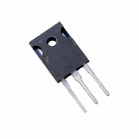
IGBT N-CH SMPS 600V 75A TO247

FGH40N6S2D

Manufacturer Part Number
FGH40N6S2D
Description
IGBT N-CH SMPS 600V 75A TO247
Manufacturer
Fairchild Semiconductor
Datasheet

Specifications of FGH40N6S2D

Voltage - Collector Emitter Breakdown (max)
600V
Vce(on) (max) @ Vge, Ic
2.7V @ 15V, 20A
Current - Collector (ic) (max)
75A
Power - Max
290W
Input Type
Standard
Mounting Type
Through Hole
Package / Case
TO-247-3
Lead Free Status / RoHS Status
Lead free / RoHS Compliant
Igbt Type
-
Other names
FGH40N6S2D_NL
FGH40N6S2D_NL

Available stocks

Company
Part Number
Manufacturer
Quantity
Price
Part Number:
FGH40N6S2D
Manufacturer:
FSC
Quantity:
6 000
©2002 Fairchild Semiconductor Corporation
FGH40N6S2D
600V, SMPS II Series N-Channel IGBT with Anti-Parallel Stealth
General Description
The FGH40N6S2D is a Low Gate Charge, Low Plateau
Voltage SMPS II IGBT combining the fast switching speed
of the SMPS IGBTs along with lower gate charge, plateau
voltage and avalanche capability (UIS). These LGC devices
shorten delay times, and reduce the power requirement of
the gate drive. These devices are ideally suited for high volt-
age switched mode power supply applications where low
conduction loss, fast switching times and UIS capability are
essential. SMPS II LGC devices have been specially de-
signed for:
IGBT (co-pack) formerly Developmental Type TA49340
Diode formerly Developmental Type TA49391
Device Maximum Ratings
Package
NOTE:
1. Pulse width limited by maximum junction temperature.
CAUTION: Stresses above those listed in “Absolute Maximum Ratings” may cause permanent damage to the device. This is a stress only rating and
• Power Factor Correction (PFC) circuits
• Full bridge topologies
• Half bridge topologies
• Push-Pull circuits
• Uninterruptible power supplies
• Zero voltage and zero current switching circuits
Symbol
BV
SSOA
operation of the device at these or any other conditions above those indicated in the operational sections of this specification is not implied.
V
I
V
T
I
E
C110
I
C25
GEM
P
GES
T
STG
CM
CES
AS
D
J
Collector to Emitter Breakdown Voltage
Collector Current Continuous, T
Collector Current Pulsed (Note 1)
Gate to Emitter Voltage Continuous
Gate to Emitter Voltage Pulsed
Switching Safe Operating Area at T
Pulsed Avalanche Energy, I
Power Dissipation Total T
Power Dissipation Derating T
Operating Junction Temperature Range
Storage Junction Temperature Range
JEDEC STYLE TO-247
C
T
= 25°C
CE
C
= 25°C unless otherwise noted
C
= 30A, L = 1mH, V
> 25°C
C
C
Parameter
= 25°C
= 110°C
J
= 150°C, Figure 2
E
(BOTTOM SIDE
COLLECTOR
Features
• 100kHz Operation at 390V, 24A
• 200kHZ Operation at 390V, 18A
• 600V Switching SOA Capability
• Typical Fall Time. . . . . . . . . . . 85ns at TJ = 125
• Low Gate Charge . . . . . . . . . 35nC at V
• Low Plateau Voltage . . . . . . . . . . . . .6.5V Typical
• UIS Rated . . . . . . . . . . . . . . . . . . . . . . . . . 260mJ
• Low Conduction Loss
C
DD
METAL)
G
= 50V
100A at 600V
-55 to 150
-55 to 150
Ratings
2.33
600
180
±20
±30
260
290
TM
75
35
G
Diode
Symbol
Juiy 2002
FGH40N6S2D RevA3
GE
C
E
Units
W/°C
= 15V
mJ
°C
°C
W
V
A
A
A
V
V
o
C

Related parts for FGH40N6S2D

FGH40N6S2D Summary of contents

Page 1

... FGH40N6S2D 600V, SMPS II Series N-Channel IGBT with Anti-Parallel Stealth General Description The FGH40N6S2D is a Low Gate Charge, Low Plateau Voltage SMPS II IGBT combining the fast switching speed of the SMPS IGBTs along with lower gate charge, plateau voltage and avalanche capability (UIS). These LGC devices shorten delay times, and reduce the power requirement of the gate drive ...

Page 2

... N/A 30 Min Typ Max Units 600 - - 250 2 ±250 nA - 1.9 2 1.7 2 2.2 2 3.5 4.3 5 6.5 8 100 - - 115 - J - 200 - J - 195 260 105 ns - 115 - J - 380 450 J - 375 600 0.43 °C 1.25 °C/W is the turn-on loss ON1 = 0A). All devices were tested per CE FGH40N6S2D RevA3 J ...

Page 3

... V , COLLECTOR TO EMITTER VOLTAGE ( 390V 125 GATE TO EMITTER VOLTAGE (V) GE =15V 150 125 J 0.4 0.6 0.8 1.0 1.2 1.4 1.6 1.8 2.0 2.2 2 COLLECTOR TO EMITTER VOLTAGE (V) CE FGH40N6S2D RevA3 700 500 450 400 350 300 250 ...

Page 4

... L = 200 390V 125 10V 15V 10V COLLECTOR TO EMITTER CURRENT (A) CE Emitter Current = 200 390V 125 10V 125 COLLECTOR TO EMITTER CURRENT (A) CE Emitter Current = 200 390V 125 10V 10V COLLECTOR TO EMITTER CURRENT (A) CE Current FGH40N6S2D RevA3 = 15V 35 40 =15V 15V = 15V 35 40 ...

Page 5

... Figure 18. Collector to Emitter On-State Voltage vs = 1mA 600V 400V 200V GATE CHARGE (nC) G Figure 14. Gate Charge o = 125 200 390V 15V TOTAL ON2 OFF I = 40A 20A 10A CE 10 100 R , GATE RESISTANCE ( ) G Resistance I = 40A 20A 10A GATE TO EMITTER VOLTAGE (V) GE Gate to Emitter Voltage FGH40N6S2D RevA3 30 35 1000 15 16 ...

Page 6

... 20A EC o 125 10A 20A 10A EC 300 400 500 600 700 800 900 dI /dt, RATE OF CHANGE OF CURRENT ( Current o = 390V 125 20A 10A EC 300 400 500 600 700 800 900 dI /dt, CURRENT RATE OF CHANGE ( Rate of Change of Current FGH40N6S2D RevA3 1000 1000 ...

Page 7

... Test Circuit and Waveforms L = 200 FGH40N6S2D Figure 26. Inductive Switching Test Circuit ©2002 Fairchild Semiconductor Corporation T = 25°C unless otherwise noted RECTANGULAR PULSE DURATION (s) 1 FGH40N6S2D DIODE TA49391 390V DD - Figure 27. Switching Test Waveforms DUTY FACTOR PEAK 90% 10% E ON2 E OFF 90% 10% t d(OFF d(ON)I FGH40N6S2D RevA3 1 10 ...

Page 8

... E collector current equals zero (I ECCOSORBD is a Trademark of Emerson and Cumming, Inc. ) plots are CE = 0.05/( d(OFF)I d(ON)I and t are d(OFF)I d(ON important JM d(OFF )/( OFF ON2 ) is defined 50 )/ the integral of ON2 during turn i.e., the OFF = 0) CE FGH40N6S2D RevA3 ...

Page 9

... TRADEMARKS The following are registered and unregistered trademarks Fairchild Semiconductor owns or is authorized to use and is not intended exhaustive list of all such trademarks. ACEx™ FASTr™ Bottomless™ FRFET™ GlobalOptoisolator™ CoolFET™ GTO™ CROSSVOLT™ HiSeC™ DOME™ ...

Related keywords