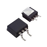
HGT1S7N60C3DS Fairchild Semiconductor, HGT1S7N60C3DS Datasheet

HGT1S7N60C3DS
Specifications of HGT1S7N60C3DS
Available stocks
Related parts for HGT1S7N60C3DS
HGT1S7N60C3DS Summary of contents
Page 1
... HGTP7N60C3D, HGT1S7N60C3DS, HGT1S7N60C3D 14A, 600V, UFS Series N-Channel IGBT with Anti-Parallel Hyperfast Diodes General Description The HGTP7N60C3D, HGT1S7N60C3DS HGT1S7N60C3D are MOS gated high voltage switching devices combining the best features of MOSFETs and bipolar transistors. These devices have the high input impedance of a MOSFET and the low on-state conduction loss of a bipolar transistor ...
Page 2
... Thermal Resistance Diode Package Marking and Ordering Information Part Number HGTP7N60C3D HGT1S7N60C3DS HGT1S7N60C3D NOTES:When ordering, use the entire part number. Add the suffix 9A to obtain the TO-263AB variant in tape and reel, i.e. HGT1S7N60C3DS9A. HGTP7N60C3D, HGT1S7N60C3DS, HGT1S7N60C3D Rev 25°C unless otherwise noted A ...
Page 3
... C110 V = 0.8 BV CE(PK) CES V = 15V 50Ω 1mH V = 15V C110 20V CE CES 7A, dI /dt = 200A/µ 1A, dI /dt = 200A/µ 0A). The HGTP7N60C3D and HGT1S7N60C3DS were tested per JEDEC CE 3 Min Typ Max Units 600 - - V µA 250 - - 2.0 mA ±250 - - 1.6 2 1.9 2.4 V 3.0 5.0 6 ...
Page 4
... DUTY CYCLE <0.5 10V - COLLECTOR TO EMITTER VOLTAGE (V) CE Figure 3. COLLECTOR TO EMITTER ON-STATE VOLTAGE 100 T , CASE TEMPERATURE ( C Figure 5. MAXIMUM DC COLLECTOR CURRENT vs CASE TEMPERATURE HGTP7N60C3D, HGT1S7N60C3DS, HGT1S7N60C3D Rev PULSE DURATION = 250µs, DUTY CYCLE <0.5 Figure 2. 40 PULSE DURATION = 250µs DUTY CYCLE <0.5 150 ...
Page 5
... TURN-ON RISE TIME vs COLLECTOR TO EMITTER CURRENT 2000 150 50Ω 1mH CE(PK) 1000 500 100 COLLECTOR TO EMITTER CURRENT (A) CE Figure 11. TURN-ON ENERGY LOSS vs COLLECTOR TO EMITTER CURRENT HGTP7N60C3D, HGT1S7N60C3DS, HGT1S7N60C3D Rev 500 T = 150 = 480V J 450 400 350 300 250 200 Figure 8. COLLECTOR TO EMITTER CURRENT 300 150 ...
Page 6
... RES COLLECTOR TO EMITTER VOLTAGE (V) CE Figure 15. CAPACITANCE vs COLLECTOR TO EMITTER VOLTAGE 0 10 0.5 0.2 0 0.05 0.02 0.01 SINGLE PULSE - Figure 17. IGBT NORMALIZED TRANSIENT THERMAL IMPEDANCE, JUNCTION TO CASE HGTP7N60C3D, HGT1S7N60C3DS, HGT1S7N60C3D Rev 150 50Ω 1mH 15V 100 CE(PK) Figure 14. MINIMUM SWITCHING SAFE 600 ...
Page 7
... C 1.0 0.5 0 0.5 1.0 1 FORWARD VOLTAGE (V) EC Figure 18. DIODE FORWARD CURRENT vs FORWARD VOLTAGE DROP Test Circuit and Waveforms L = 1mH RHRD660 R = 50Ω G Figure 20. INDUCTIVE SWITCHING TEST CIRCUIT HGTP7N60C3D, HGT1S7N60C3DS, HGT1S7N60C3D Rev 2.5 2.0 3.0 0.5 Figure 19. RECOVERY TIMES vs FORWARD V GE ...
Page 8
... Gate Protection - These devices do not have an internal monolithic zener diode from gate to emitter. If gate protection is required an external zener is recommended. HGTP7N60C3D, HGT1S7N60C3DS, HGT1S7N60C3D Rev Operating Frequency Information Operating frequency information for a typical device (Figure 13) is presented as a guide for estimating device performance for a specific application ...
Page 9
... PRODUCT STATUS DEFINITIONS Definition of Terms Datasheet Identification Advance Information Preliminary No Identification Needed Obsolete HGTP7N60C3D, HGT1S7N60C3DS, HGT1S7N60C3D Rev i-Lo™ PACMAN™ ImpliedDisconnect™ POP™ IntelliMAX™ Power247™ ISOPLANAR™ ...


