FDG8842CZ Fairchild Semiconductor, FDG8842CZ Datasheet
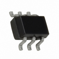
MOSFET N/P-CH 30V/-25V SC70-6

FDG8842CZ

Manufacturer Part Number
FDG8842CZ
Description
MOSFET N/P-CH 30V/-25V SC70-6
Manufacturer
Fairchild Semiconductor
Series
PowerTrench®r
Datasheet

Specifications of FDG8842CZ

Fet Type
N and P-Channel
Fet Feature
Logic Level Gate
Rds On (max) @ Id, Vgs
400 mOhm @ 750mA, 4.5V
Drain To Source Voltage (vdss)
30V, 25V
Current - Continuous Drain (id) @ 25° C
750mA, 410mA
Vgs(th) (max) @ Id
1.5V @ 250µA
Gate Charge (qg) @ Vgs
1.44nC @ 4.5V
Input Capacitance (ciss) @ Vds
120pF @ 10V
Power - Max
300mW
Mounting Type
Surface Mount
Package / Case
SC-70-6, SC-88, SOT-363
Lead Free Status / RoHS Status
Lead free / RoHS Compliant
Other names
FDG8842CZTR

Available stocks

Company
Part Number
Manufacturer
Quantity
Price
Part Number:
FDG8842CZ
Manufacturer:
FSC
Quantity:
36 000
Part Number:
FDG8842CZ
Manufacturer:
FAIRCHILD
Quantity:
2 754
Part Number:
FDG8842CZ
Manufacturer:
FSC
Quantity:
3 000
Part Number:
FDG8842CZ
Manufacturer:
FAIRCHILD/仙童
Quantity:
20 000
Part Number:
FDG8842CZ
0
Company:
Part Number:
FDG8842CZ
Quantity:
4 500
Company:
Part Number:
FDG8842CZ
Quantity:
200
Part Number:
FDG8842CZ-NL
Manufacturer:
DIODES/美台
Quantity:
20 000
Part Number:
FDG8842CZ_NL
Manufacturer:
FAIRCHILD/仙童
Quantity:
20 000
©2007 Fairchild Semiconductor Corporation
FDG8842CZ Rev.B
FDG8842CZ
Complementary PowerTrench
Q1:30V,0.75A,0.4Ω; Q2:–25V,–0.41A,1.1Ω
Features
Q1: N-Channel
Q2: P-Channel
MOSFET Maximum Ratings
Thermal Characteristics
Package Marking and Ordering Information
V
V
I
P
T
R
R
D
DS
GS
D
J
θJA
θJA
Max r
Max r
Max r
Max r
Very low level gate drive requirements allowing direct
operation in 3V circuits(V
Very small package outline SC70-6
RoHS Compliant
, T
Symbol
Device Marking
STG
DS(on)
DS(on)
DS(on)
DS(on)
.42
= 0.4Ω at V
= 0.5Ω at V
= 1.1Ω at V
= 1.5Ω at V
SC70-6
Drain to Source Voltage
Gate to Source Voltage
Drain Current
Power Dissipation for Single Operation
Operating and Storage Junction Temperature Range
Thermal Resistance, Junction to Ambient Single operation
D1
GS
GS
GS
GS
GS(th)
G2
= 4.5V, I
= 2.7V, I
= –4.5V, I
= –2.7V, I
Pin 1
<1.5V)
S2
FDG8842CZ
-Continuous
D
D
-Pulsed
Device
D
D
= 0.75A
= 0.67A
= –0.41A
= –0.25A
S1
T
A
= 25°C unless otherwise noted
G1
Parameter
D2
®
MOSFET
1
Reel Size
General Description
These N & P-Channel logic level enhancement mode field effect
transistors are produced using Fairchild’s proprietary, high cell
density, DMOS technology. This very high density process is
especially
device has been designed especially for low voltage applica-
tions as a replacement for bipolar digital transistors and small
signal MOSFETs. Since bias resistors are not required, this dual
digital FET can replace several different digital transistors, with
different bias resistor values.
7”
S1
G1
D2
tailored
(Note 1a)
(Note 1b)
(Note 1a)
(Note 1b)
Q1
Q2
to minimize on-state resistance.
Tape Width
8mm
0.75
±12
Q1
2.2
30
–55 to +150
0.36
0.30
350
415
–0.41
G2
D1
S2
–1.2
–25
Q2
–8
April 2007
www.fairchildsemi.com
3000 units
Quantity
Units
°C/W
°C
W
V
V
A
This
tm

Related parts for FDG8842CZ

FDG8842CZ Summary of contents

Page 1

... Thermal Resistance, Junction to Ambient Single operation θJA Package Marking and Ordering Information Device Marking .42 ©2007 Fairchild Semiconductor Corporation FDG8842CZ Rev.B ® MOSFET General Description These N & P-Channel logic level enhancement mode field effect transistors are produced using Fairchild’s proprietary, high cell = 0 ...

Page 2

... Turn-Off Delay Time d(off) t Fall Time f Q Total Gate Charge g Q Gate to Source Charge gs Q Gate to Drain “Miller” Charge gd ©2007 Fairchild Semiconductor Corporation FDG8842CZ Rev 25°C unless otherwise noted J Test Conditions I = 250μ –250μ 250μA, referenced to 25°C ...

Page 3

... R is determined by the user's board design. θJC θJA a. 350°C/W when mounted Scale 1:1 on letter size paper. 2. Pulse Test: Pulse Width < 300μs, Duty cycle < 2.0%. ©2007 Fairchild Semiconductor Corporation FDG8842CZ Rev 25°C unless otherwise noted J Test Conditions 0.3A GS ...

Page 4

... PULSE DURATION = 80 μ s DUTY CYCLE = 0.5%MAX 1.76 VDD = 5V 1.32 0. 150 J 0.44 0.00 0.0 0.5 1 GATE TO SOURCE VOLTAGE (V) GS Figure 5. Transfer Characteristics ©2007 Fairchild Semiconductor Corporation FDG8842CZ Rev 25°C unless otherwise noted J 2 2.0V GS 2.2 1.8 V =1.8V GS 1.4 μ 1.5V GS 0.6 1 ...

Page 5

... DS Figure 9. Forward Bias Safe Operating Area 1 DUTY CYCLE-DESCENDING ORDER D = 0.5 0.2 0.1 0.05 0.02 0.1 0.01 SINGLE PULSE 0.01 0.0001 0.001 ©2007 Fairchild Semiconductor Corporation FDG8842CZ Rev 25°C unless otherwise noted 10V 15V DD 0.8 1.0 1.2 1.4 100 μ s 1ms 10ms ...

Page 6

... Figure 15. Normalized On Resistance vs Junction Temperature 0.6 PULSE DURATION = 80 μ s DUTY CYCLE = 0.5%MAX -5V DS 0.4 0.2 0.0 0.5 1.0 1 GATE TO SOURCE VOLTAGE (V) GS Figure 17. Transfer Characteristics ©2007 Fairchild Semiconductor Corporation FDG8842CZ Rev 25°C unless otherwise noted -2. -2. -2.0V GS μ -1. Figure 14. Normalized on-Resistance vs Drain ...

Page 7

... DRAIN to SOURCE VOLTAGE (V) DS Figure 21. Forward Bias Safe Operating Area 1 DUTY CYCLE-DESCENDING ORDER D = 0.5 0.2 0.1 0.05 0.02 0.01 0.1 SINGLE PULSE 0. ©2007 Fairchild Semiconductor Corporation FDG8842CZ Rev 25°C unless otherwise noted -10V DD = -15V DD 1.2 1.6 1ms 10ms 100ms RECTANGULAR PULSE DURATION (s) Figure 23 ...

Page 8

... TRADEMARKS The following are registered and unregistered trademarks Fairchild Semiconductor owns or is authorized to use and is not intended exhaustive list of all such trademarks. ® ACEx Across the board. Around the world™ ActiveArray™ Bottomless™ Build it Now™ CoolFET™ CROSSVOLT™ ...

Related keywords