FDG8850NZ Fairchild Semiconductor, FDG8850NZ Datasheet
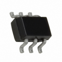
MOSFET DUAL N-CH 30V SC70-6

FDG8850NZ

Manufacturer Part Number
FDG8850NZ
Description
MOSFET DUAL N-CH 30V SC70-6
Manufacturer
Fairchild Semiconductor
Series
PowerTrench®r
Datasheet

Specifications of FDG8850NZ

Fet Type
2 N-Channel (Dual)
Fet Feature
Logic Level Gate
Rds On (max) @ Id, Vgs
400 mOhm @ 750mA, 4.5V
Drain To Source Voltage (vdss)
30V
Current - Continuous Drain (id) @ 25° C
750mA
Vgs(th) (max) @ Id
1.5V @ 250µA
Gate Charge (qg) @ Vgs
1.44nC @ 4.5V
Input Capacitance (ciss) @ Vds
120pF @ 10V
Power - Max
300mW
Mounting Type
Surface Mount
Package / Case
SC-70-6, SC-88, SOT-363
Configuration
Dual
Transistor Polarity
N-Channel
Resistance Drain-source Rds (on)
0.4 Ohm @ 4.5 V
Drain-source Breakdown Voltage
30 V
Gate-source Breakdown Voltage
+/- 12 V
Continuous Drain Current
0.75 A
Power Dissipation
360 mW
Maximum Operating Temperature
+ 150 C
Mounting Style
SMD/SMT
Minimum Operating Temperature
- 55 C
Module Configuration
Dual
Continuous Drain Current Id
750mA
Drain Source Voltage Vds
30V
On Resistance Rds(on)
250mohm
Rds(on) Test Voltage Vgs
4.5V
Rohs Compliant
Yes
Lead Free Status / RoHS Status
Lead free / RoHS Compliant
Other names
FDG8850NZTR

Available stocks

Company
Part Number
Manufacturer
Quantity
Price
Part Number:
FDG8850NZ
Manufacturer:
FAIRCHILD
Quantity:
20 000
Part Number:
FDG8850NZ
Manufacturer:
FSC进口
Quantity:
20 000
Part Number:
FDG8850NZ
0
Company:
Part Number:
FDG8850NZ
Quantity:
3 000
©2007 Fairchild Semiconductor Corporation
FDG8850NZ Rev.B
FDG8850NZ
Dual N-Channel PowerTrench
30V,0.75A,0.4Ω
Features
MOSFET Maximum Ratings
Thermal Characteristics
Package Marking and Ordering Information
V
V
I
P
T
R
R
D
DS
GS
D
J
θJA
θJA
Max r
Max r
Very low level gate drive requirements allowing operation
in 3V circuits(V
Very small package outline SC70-6
RoHS Compliant
, T
Symbol
Device Marking
STG
DS(on)
DS(on)
.50
= 0.4Ω at V
= 0.5Ω at V
SC70-6
GS(th)
Drain to Source Voltage
Gate to Source Voltage
Drain Current
Power Dissipation for Single Operation
Operating and Storage Junction Temperature Range
Thermal Resistance, Junction to Ambient Single operation
D1
<1.5V)
GS
GS
G2
= 4.5V, I
= 2.7V, I
Pin 1
S2
FDG8850NZ
-Continuous
D
D
-Pulsed
Device
= 0.75A
= 0.67A
S1
T
A
= 25°C unless otherwise noted
G1
Parameter
D2
®
MOSFET
1
Reel Size
General Description
This dual N-Channel logic level enhancement mode field effect
transistors are produced using Fairchild’s proprietary, high cell
density, DMOS technology. This very high density process is
especially tailored to minimize on-state resistance. This device
has been designed especially for low voltage applications as
a replacement for bipolar digital transistors and small signal
MOSFETs. Since bias resistors are not required, this dual digital
FET can replace several different digital transistors, with differ-
ent bias resistor values.
7”
S1
G1
D2
(Note 1a)
(Note 1b)
(Note 1a)
(Note 1b)
Q1
Q2
Tape Width
8mm
–55 to +150
Ratings
0.75
0.36
0.30
350
415
±12
2.2
30
April 2007
D1
www.fairchildsemi.com
G2
S2
3000 units
Quantity
Units
°C/W
°C
W
V
V
A
tm

Related parts for FDG8850NZ

FDG8850NZ Summary of contents

Page 1

... R Thermal Resistance, Junction to Ambient Single operation θJA Package Marking and Ordering Information Device Marking .50 ©2007 Fairchild Semiconductor Corporation FDG8850NZ Rev.B ® MOSFET General Description This dual N-Channel logic level enhancement mode field effect = 0.75A D transistors are produced using Fairchild’s proprietary, high cell = 0 ...

Page 2

... R is determined by the user's board design. θJC θJA a. 350°C/W when mounted Scale 1:1 on letter size paper. 2. Pulse Test: Pulse Width < 300μs, Duty cycle < 2.0%. ©2007 Fairchild Semiconductor Corporation FDG8850NZ Rev 25°C unless otherwise noted J Test Conditions I = 250μ 250μ ...

Page 3

... PULSE DURATION = 80 μ s DUTY CYCLE = 0.5%MAX 1.76 VDD = 5V 1.32 0. 150 J 0.44 0.00 0.0 0.5 1 GATE TO SOURCE VOLTAGE (V) GS Figure 5. Transfer Characteristics ©2007 Fairchild Semiconductor Corporation FDG8850NZ Rev 25°C unless otherwise noted J 2 2.0V GS 2.2 1.8 V =1.8V GS 1.4 μ 1.5V GS 0.6 1 ...

Page 4

... DS Figure 9. Forward Bias Safe Operating Area 1 DUTY CYCLE-DESCENDING ORDER D = 0.5 0.2 0.1 0.05 0.02 0.1 0.01 SINGLE PULSE 0.01 0.0001 0.001 ©2007 Fairchild Semiconductor Corporation FDG8850NZ Rev 25°C unless otherwise noted 10V 15V DD 0.8 1.0 1.2 1.4 100 μ s 1ms 10ms ...

Page 5

... TRADEMARKS The following are registered and unregistered trademarks Fairchild Semiconductor owns or is authorized to use and is not intended exhaustive list of all such trademarks. ® ACEx Across the board. Around the world™ ActiveArray™ Bottomless™ Build it Now™ CoolFET™ CROSSVOLT™ ...

Related keywords