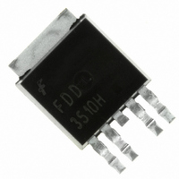
FDD3510H Fairchild Semiconductor, FDD3510H Datasheet

FDD3510H
Specifications of FDD3510H
Available stocks
Related parts for FDD3510H
FDD3510H Summary of contents
Page 1
... Thermal Resistance, Junction to Case, Single Operation for Q2 θJC Package Marking and Ordering Information Device Marking Device FDD3510H FDD3510H ©2008 Fairchild Semiconductor Corporation FDD3510H Rev.C ® MOSFET General Description These dual N and P-Channel enhancement MOSFETs are produced using Fairchild Semiconductor’s = 4.3A D advanced PowerTrench = 4 ...
Page 2
... Rise Time r t Turn-Off Delay Time d(off) t Fall Time f Q Total Gate Charge g(TOT) Q Gate to Source Charge gs Q Gate to Drain “Miller” Charge gd FDD3510H Rev 25°C unless otherwise noted J Test Conditions I =250µ -250µ 250µA, referenced to 25° -250µ ...
Page 3
... Q Reverse Recovery Charge rr Notes determined with the device mounted on a 1in θJA by the user's board design Pulse Test: Pulse Width < 300µs, Duty cycle < 2.0%. 3. Starting T = 25°C, N-ch 3mH 5A FDD3510H Rev 25°C unless otherwise noted J Test Conditions -2. ...
Page 4
... JUNCTION TEMPERATURE ( , T J Figure 3. Normalized On Resistance vs Junction Temperature 20 µ PULSE DURATION = 80 s DUTY CYCLE = 0.5%MAX 150 GATE TO SOURCE VOLTAGE (V) GS Figure 5. Transfer Characteristics FDD3510H Rev 25°C unless otherwise noted 4.5V GS µ PULSE DURATION = X s DUTY CYCLE = X%MAX 3. 100 125 150 ...
Page 5
... Unclamped Inductive Switching Capability 50 10 THIS AREA IS LIMITED DS(on) SINGLE PULSE T = MAX RATED 3.5 C/W θ 0.05 0 DRAIN to SOURCE VOLTAGE (V) DS Figure 11. Forward Bias Safe Operating Area FDD3510H Rev 25°C unless otherwise noted J 1000 V = 50V 100 100us 10 1ms 10 10ms 100ms DC ...
Page 6
... DUTY CYCLE-DESCENDING ORDER D = 0.5 0.2 0.1 0.1 0.05 0.02 0.01 0.01 0.001 - FDD3510H Rev 25°C unless otherwise noted J SINGLE PULSE 3.5 C/W θ RECTANGULAR PULSE DURATION (sec) Figure 13. Transient Thermal Response Curve SINGLE PULSE C/W θ ...
Page 7
... PULSE DURATION = 80 s DUTY CYCLE = 0.5%MAX - 150 GATE TO SOURCE VOLTAGE (V) GS Figure 19. Transfer Characteristics FDD3510H Rev 25°C unless otherwise noted J = -4. -3.5V GS µ PULSE DURATION = 80 s DUTY CYCLE = 0.5%MAX -2. Figure 16. Normalized on-Resistance vs Drain 600 500 400 300 200 100 50 ...
Page 8
... Switching Capability THIS AREA IS LIMITED BY r ds(on) SINGLE PULSE T = MAX RATED 3.9 C/W θ DRAIN to SOURCE VOLTAGE (V) DS Figure 25. Forward Bias Safe Operating Area FDD3510H Rev 25°C unless otherwise noted -50V 100us 1ms 10ms 100ms DC 100 200 8 1000 100 f = 1MHz ...
Page 9
... R = 3.9 θ JC 0.001 - DUTY CYCLE-DESCENDING ORDER D = 0.5 0.2 0.1 0.1 0.05 0.02 0.01 0.01 0.001 - FDD3510H Rev 25°C unless otherwise noted J C RECTANGULAR PULSE DURATION (s) Figure 27. Transient Thermal Response Curve SINGLE PULSE C/W θ Note RECTANGULAR PULSE DURATION (sec) Figure 28. Transient Thermal Response Curve ...
Page 10
... Definition of Terms Datasheet Identification Product Status Advance Information Formative or In Design Preliminary First Production No Identification Needed Full Production Obsolete Not In Production FDD3510H Rev.C Preliminary Datasheet FPS™ PDP-SPM™ F-PFS™ Power-SPM™ ® FRFET PowerTrench SM Global Power Resource Programmable Active Droop™ ...


