FDP038AN06A0 Fairchild Semiconductor, FDP038AN06A0 Datasheet - Page 2
FDP038AN06A0
Manufacturer Part Number
FDP038AN06A0
Description
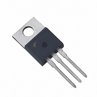
MOSFET N-CH 60V 80A TO-220AB
Manufacturer
Fairchild Semiconductor
Series
PowerTrench®r
Datasheet
1.FDI038AN06A0.pdf
(10 pages)
Specifications of FDP038AN06A0
Fet Type
MOSFET N-Channel, Metal Oxide
Fet Feature
Standard
Rds On (max) @ Id, Vgs
3.8 mOhm @ 80A, 10V
Drain To Source Voltage (vdss)
60V
Current - Continuous Drain (id) @ 25° C
80A
Vgs(th) (max) @ Id
4V @ 250µA
Gate Charge (qg) @ Vgs
124nC @ 10V
Input Capacitance (ciss) @ Vds
6400pF @ 25V
Power - Max
310W
Mounting Type
Through Hole
Package / Case
TO-220-3 (Straight Leads)
Configuration
Single
Transistor Polarity
N-Channel
Resistance Drain-source Rds (on)
0.0038 Ohm @ 10 V
Drain-source Breakdown Voltage
60 V
Gate-source Breakdown Voltage
+/- 20 V
Continuous Drain Current
17 A
Power Dissipation
310000 mW
Maximum Operating Temperature
+ 175 C
Mounting Style
Through Hole
Minimum Operating Temperature
- 55 C
Lead Free Status / RoHS Status
Lead free / RoHS Compliant
Available stocks
Company
Part Number
Manufacturer
Quantity
Price
Company:

Part Number:
FDP038AN06A0
Manufacturer:
FSC
Quantity:
18 000
Company:
Part Number:
FDP038AN06A0
Manufacturer:
FAIRCHILD
Quantity:
12 500
Part Number:
FDP038AN06A0
Manufacturer:
FAIRCHILD/仙童
Quantity:
20 000


©2010 Fairchild Semiconductor Corporation
Package Marking and Ordering Information
Electrical Characteristics
Off Characteristics
On Characteristics
Dynamic Characteristics
Switching Characteristics
Drain-Source Diode Characteristics
Notes:
1: Starting T
2: Pulse Width = 100s
B
I
I
V
r
C
C
C
Q
Q
Q
Q
Q
t
t
t
t
t
t
V
t
Q
DSS
GSS
ON
d(ON)
r
d(OFF)
f
OFF
rr
DS(ON)
GS(TH)
VDSS
SD
ISS
OSS
RSS
g(TOT)
g(TH)
gs
gs2
gd
RR
Symbol
FDP038AN06A0
Device Marking
FDI038AN06A0
J
= 25°C, L = 0.255mH, I
Drain to Source Breakdown Voltage
Zero Gate Voltage Drain Current
Gate to Source Leakage Current
Gate to Source Threshold Voltage
Drain to Source On Resistance
Input Capacitance
Output Capacitance
Reverse Transfer Capacitance
Total Gate Charge at 10V
Threshold Gate Charge
Gate to Source Gate Charge
Gate Charge Threshold to Plateau
Gate to Drain “Miller” Charge
Turn-On Time
Turn-On Delay Time
Rise Time
Turn-Off Delay Time
Fall Time
Turn-Off Time
Source to Drain Diode Voltage
Reverse Recovery Time
Reverse Recovered Charge
AS
FDP038AN06A0
Parameter
FDI038AN06A0
= 70A.
Device
(V
GS
= 10V)
T
C
= 25°C unless otherwise noted
TO-220AB
TO-262AB
Package
I
V
V
V
V
I
I
I
T
V
f = 1MHz
V
V
V
V
I
I
I
I
D
D
D
D
SD
SD
SD
SD
J
DS
GS
GS
GS
DS
GS
GS
DD
GS
= 250 A, V
= 80A, V
= 40A, V
= 80A, V
= 175
= 80A
= 40A
= 75A, dI
= 75A, dI
= 50V
= 0V
= 20V
= V
= 25V, V
= 0V to 10V
= 0V to 2V
= 30V, I
= 10V, R
Test Conditions
DS
o
C
, I
GS
GS
GS
D
D
SD
SD
GS
GS
GS
= 80A
= 10V
= 6V
= 10V,
= 250 A
/dt = 100A/ s
/dt = 100A/ s
Reel Size
= 0V,
= 0V
= 2.4
T
V
I
I
D
g
Tube
Tube
C
DD
= 1.0mA
= 80A
= 150
= 30V
o
C
Tape Width
Min
60
2
-
-
-
-
-
-
-
-
-
-
-
-
-
-
-
-
-
-
-
-
-
-
-
N/A
N/A
0.0035 0.0038
0.0049 0.0074
0.0071 0.0078
6400
1123
367
144
Typ
FDP038AN06A0 / FDI038AN06A0 Rev. B2
96
12
26
15
27
17
34
60
-
-
-
-
-
-
-
-
-
-
-
1.25
Max
250
124
175
115
1.0
100
15
38
39
Quantity
1
4
-
-
-
-
-
-
-
-
-
-
-
50 units
50 units
Units
nC
nC
nC
nC
nC
nC
nA
pF
pF
pF
ns
ns
ns
ns
ns
ns
ns
V
V
V
V
A
Related parts for FDP038AN06A0
Image
Part Number
Description
Manufacturer
Datasheet
Request
R

Part Number:
Description:
Fairchild Semiconductor [IGBT MODULE]
Manufacturer:
Fairchild Semiconductor
Datasheet:

Part Number:
Description:
Discrete Semiconductor Modules
Manufacturer:
Fairchild Semiconductor
Part Number:
Description:
Discrete Semiconductor Modules
Manufacturer:
Fairchild Semiconductor
Part Number:
Description:
This N-Channel MOSFET is produced using Fairchild Semiconductor’s advanced Power Trench® process
Manufacturer:
Fairchild Semiconductor
Datasheet:
Part Number:
Description:
This N-Channel MOSFET is produced using Fairchild Semiconductor’s advanced Power Trench® process
Manufacturer:
Fairchild Semiconductor
Datasheet:
Part Number:
Description:
This N-Channel MOSFET is produced using Fairchild Semiconductor’s advanced PowerTrench® process
Manufacturer:
Fairchild Semiconductor
Datasheet:
Part Number:
Description:
This N-Channel MOSFET is produced using Fairchild Semiconductor’s advanced PowerTrench® process
Manufacturer:
Fairchild Semiconductor
Datasheet:
Part Number:
Description:
This N-Channel MOSFET is produced using Fairchild Semiconductor’s advanced Power Trench® process
Manufacturer:
Fairchild Semiconductor
Datasheet:
Part Number:
Description:
This N-Channel logic Level MOSFETs are produced using Fairchild Semiconductor‘s advanced Power Trench® process that has been special tailored to minimize the on-state resistance and yet maintain superior switching performance
Manufacturer:
Fairchild Semiconductor
Datasheet:
Part Number:
Description:
This N-Channel MOSFET is produced using Fairchild Semiconductor’s advanced Power Trench® process
Manufacturer:
Fairchild Semiconductor
Datasheet:
Part Number:
Description:
This N-Channel SyncFET™ is produced using Fairchild Semiconductor’s advanced PowerTrench® process
Manufacturer:
Fairchild Semiconductor
Datasheet:
Part Number:
Description:
This N-Channel SyncFET™ is produced using Fairchild Semiconductor’s advanced PowerTrench® process
Manufacturer:
Fairchild Semiconductor
Datasheet:
Part Number:
Description:
This N-Channel SyncFET™ is produced using Fairchild Semiconductor’s advanced PowerTrench® process
Manufacturer:
Fairchild Semiconductor
Datasheet:
Part Number:
Description:
This N-Channel logic Level MOSFETs are produced using Fairchild Semiconductor‘s advanced Power Trench® process that has been special tailored to minimize the on-state resistance and yet maintain superior switching performance
Manufacturer:
Fairchild Semiconductor
Datasheet:
Part Number:
Description:
This N-Channel MOSFET is produced using Fairchild Semiconductor’s advanced Power Trench® process that has been especially tailored to minimize the on-state resistance and yet maintain superior switching performance
Manufacturer:
Fairchild Semiconductor
Datasheet: