FCH47N60F Fairchild Semiconductor, FCH47N60F Datasheet

MOSFET N-CH 600V 47A TO-247

FCH47N60F

Manufacturer Part Number
FCH47N60F
Description
MOSFET N-CH 600V 47A TO-247
Manufacturer
Fairchild Semiconductor
Series
SuperFET™r
Datasheet

Specifications of FCH47N60F

Fet Type
MOSFET N-Channel, Metal Oxide
Fet Feature
Standard
Rds On (max) @ Id, Vgs
73 mOhm @ 23.5A, 10V
Drain To Source Voltage (vdss)
600V
Current - Continuous Drain (id) @ 25° C
47A
Vgs(th) (max) @ Id
5V @ 250µA
Gate Charge (qg) @ Vgs
270nC @ 10V
Input Capacitance (ciss) @ Vds
8000pF @ 25V
Power - Max
417W
Mounting Type
Through Hole
Package / Case
TO-247-3
Lead Free Status / RoHS Status
Lead free / RoHS Compliant

Available stocks

Company
Part Number
Manufacturer
Quantity
Price
Part Number:
FCH47N60F
Manufacturer:
FAIRCHILD
Quantity:
8 000
Part Number:
FCH47N60F
Manufacturer:
FSC/ON 可看货
Quantity:
20 000
Company:
Part Number:
FCH47N60F-F133
Quantity:
2 500
Part Number:
FCH47N60F_F133
Manufacturer:
FSC可看货
Quantity:
20 000
©2006 Fairchild Semiconductor Corporation
FCH47N60F Rev. B
FCH47N60F
600V N-Channel MOSFET
Features
• 650V @T
• Typ. R
• Fast Recovery Type ( t
• Ultra Low Gate Charge (typ. Q
• Low Effective Output Capacitance (typ. C
• 100% avalanche tested
Absolute Maximum Ratings
Thermal Characteristics
V
I
I
V
E
I
E
dv/dt
P
T
T
R
R
R
D
DM
AR
J,
L
DSS
GSS
AS
AR
D
Symbol
Symbol
θJC
θCS
θJA
T
STG
DS(on)
J
= 150°C
= 0.062Ω
Drain-Source Voltage
Drain Current
Drain Current
Gate-Source voltage
Single Pulsed Avalanche Energy
Avalanche Current
Repetitive Avalanche Energy
Peak Diode Recovery dv/dt
Power Dissipation
Maximum Lead Temperature for Soldering Purpose,
1/8” from Case for 5 Seconds
Thermal Resistance, Junction-to-Case
Thermal Resistance, Case-to-Sink
Thermal Resistance, Junction-to-Ambient
Operating and Storage Temperature Range
rr
= 240ns)
G
D
g
= 210nC)
S
- Continuous (T
- Continuous (T
- Pulsed
(T
- Derate above 25°C
Parameter
Parameter
C
= 25°C)
oss
eff. = 420pF)
TO-247
C
C
= 25°C)
= 100°C)
1
Description
SuperFET
voltage MOSFET family that is utilizing an advanced charge
balance mechanism for outstanding low on-resistance and
lower gate charge performance.
This advanced technology has been tailored
conduction loss, provide superior switching performance, and
withstand extreme dv/dt rate and higher avalanche energy.
Consequently, SuperFET is very suitable for various AC/DC
power conversion in switching mode operation for system
miniaturization and higher efficiency.
(Note 1)
(Note 2)
(Note 1)
(Note 1)
(Note 3)
TM
is, Farichild’s proprietary, new generation of high
Typ.
0.24
--
--
FCH47N60F
-55 to +150
G
1800
29.7
± 30
41.7
3.33
600
141
417
300
47
47
50
SuperFET
Max.
41.7
D
S
0.3
--
May 2006
www.fairchildsemi.com
to minimize
Unit
W/°C
V/ns
Unit
°C/W
°C/W
°C/W
mJ
mJ
°C
°C
W
V
A
A
A
V
A
TM

Related parts for FCH47N60F

FCH47N60F Summary of contents

Page 1

... R Thermal Resistance, Case-to-Sink θCS R Thermal Resistance, Junction-to-Ambient θJA ©2006 Fairchild Semiconductor Corporation FCH47N60F Rev. B Description TM SuperFET voltage MOSFET family that is utilizing an advanced charge balance mechanism for outstanding low on-resistance and lower gate charge performance. This advanced technology has been tailored conduction loss, provide superior switching performance, and eff ...

Page 2

... G J ≤ 47A, di/dt ≤ 1,200A/μs, V ≤ Starting DSS 4. Pulse Test: Pulse width ≤ 300μs, Duty Cycle ≤ Essentially Independent of Operating Temperature Typical Characteristics FCH47N60F Rev. B Package Reel Size TO-247 - T = 25°C unless otherwise noted C Conditions 250μ 25° ...

Page 3

... I , Drain Current [A] D Figure 5. Capacitance Characteristics 25000 20000 C oss 15000 C 10000 iss 5000 C rss Drain-Source Voltage [V] DS FCH47N60F Rev. B Figure 2. Transfer Characteristics Notes : 1. 250 μ s Pulse Test Figure 4. Body Diode Forward Voltage 10V 20V GS * Note : ° ...

Page 4

... ° ° 150 Single Pulse - Drain-Source Voltage [V] DS Figure 10. Transient Thermal Response Curve - FCH47N60F Rev. B (Continued) Figure 8. On-Resistance Variation 3.0 2.5 2.0 1.5 1.0 * Notes : 250 μ 0.5 0.0 100 150 200 -100 ° C] Figure 10. Maximum Drain Current 50 40 100 μ ...

Page 5

... Unclamped Inductive Switching Test Circuit & Waveforms FCH47N60F Rev. B Gate Charge Test Circuit & Waveform Resistive Switching Test Circuit & Waveforms 5 www.fairchildsemi.com ...

Page 6

... FCH47N60F Rev. B Peak Diode Recovery dv/dt Test Circuit & Waveforms 6 www.fairchildsemi.com ...

Page 7

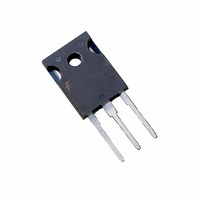
... Mechanical Dimensions TO-247AD (FKS PKG CODE 001) FCH47N60F Rev Dimensions in Millimeters www.fairchildsemi.com ...

Page 8

... PRODUCT STATUS DEFINITIONS Definition of Terms Datasheet Identification Advance Information Preliminary No Identification Needed Obsolete FCH47N60F Rev. B ISOPLANAR™ LittleFET™ MICROCOUPLER™ MicroFET™ MicroPak™ MICROWIRE™ MSX™ MSXPro™ OCX™ ...

Related keywords