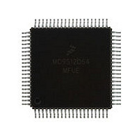
MC9S12D64MFUE Freescale, MC9S12D64MFUE Datasheet - Page 2

MC9S12D64MFUE
Manufacturer Part Number
MC9S12D64MFUE
Description
Manufacturer
Freescale
Datasheet
1.MC9S12D64MFUE.pdf
(128 pages)
Specifications of MC9S12D64MFUE
Cpu Family
HCS12
Device Core Size
16b
Frequency (max)
25MHz
Interface Type
CAN/I2C/SCI/SPI
Total Internal Ram Size
4KB
# I/os (max)
49
Number Of Timers - General Purpose
8
Operating Supply Voltage (typ)
2.5/5V
Operating Supply Voltage (max)
2.75/5.25V
Operating Supply Voltage (min)
2.35/4.5V
On-chip Adc
2(8-chx10-bit)
Instruction Set Architecture
CISC
Operating Temp Range
-40C to 125C
Operating Temperature Classification
Automotive
Mounting
Surface Mount
Pin Count
80
Package Type
PQFP
Program Memory Type
Flash
Program Memory Size
64KB
Lead Free Status / RoHS Status
Compliant
Available stocks
Company
Part Number
Manufacturer
Quantity
Price
Company:
Part Number:
MC9S12D64MFUE
Manufacturer:
Freescale Semiconductor
Quantity:
10 000
Revision History
Number
Version
V01.00
V01.01
V01.02
V01.03
V01.04
V01.05
Revision
16 NOV
18 FEB
30 July
6 MAR
4 June
Date
4 July
2001
2002
2002
2002
2002
2002
Effective
19 NOV
18 FEB
30 July
6 MAR
4 June
4 July
Date
2001
2002
2002
2002
2002
2002
Author
Initial version based on MC9SDP256-2.09 Version.
In table 7 I/O Characteristics" of the electrical characteristics
replaced tPULSE with tpign and tpval in lines "Port ... Interrupt Input
Pulse filtered" and "Port ... Interrupt Input Pulse passed"
respectively.
Table "Oscillator Characteristics": removed "Oscillator start-up time
from POR or STOP" row
Table "5V I/O Characteristics": Updated
Partial Drive IOH = +–2mA and Full Drive IOH = –10mA
Table "ATD Operating Characteristics": Distinguish I
ATD blocks on
Table "ATD Electrical Characteristics": Update C
Table "Operating Conditions": Changed V
(min)
Removed Document number except from Cover Sheet
Updated Table "Document References"
Table "5V I/O Characteristics" : Corrected Input Capacitance to 6pF
Section: "Device Pinout" (112-pin and 80-pin): added in diagrams
RXCAN0 to PJ6 and TXCAN0 to PJ7
Table "PLL Characteristics": Updated parameters K
Figure "Basic PLL functional diagram": Inserted XFC pin in diagram
Enhanced section "XFC Component Selection"
Added to Sections ATD, ECT and PWM: freeze mode = active BDM
mode
Added 1L86D to Table "Assigned Part ID numbers"
Corrected MEMSIZ1 value in Table "Memory size registers"
Subsection "Device Memory Map: Removed Flash mapping from
$0000 to $3FFF.
Table "Signal Properties": Added column "Internal Pull Resistor".
Preface Table "Document References": Changed to full naming for
each block.
Table "Interrupt Vector Locations", Column "Local Enable":
Corrected several register and bit names.
Figure "Recommended PCB Layout for 80QFP: Corrected
VREGEN pin position
Thermal values for junction to board and package
BGND pin pull-up
Part Order Information
Global Register Table
Chip Configuration Summary
Modified mode of Operations chapter
Section "Printed Circuit Board Layout Proposals": added Pierce
Oscillator examples for 112LQFP and 80QFP
Description of Changes
DD
and V
INS
DDPLL
1
REF
to 22 pF
and f
for 1 and 2
to 2.35 V
1


