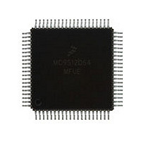
MC9S12D64MFUE Freescale, MC9S12D64MFUE Datasheet - Page 69

MC9S12D64MFUE
Manufacturer Part Number
MC9S12D64MFUE
Description
Manufacturer
Freescale
Datasheet
1.MC9S12D64MFUE.pdf
(128 pages)
Specifications of MC9S12D64MFUE
Cpu Family
HCS12
Device Core Size
16b
Frequency (max)
25MHz
Interface Type
CAN/I2C/SCI/SPI
Total Internal Ram Size
4KB
# I/os (max)
49
Number Of Timers - General Purpose
8
Operating Supply Voltage (typ)
2.5/5V
Operating Supply Voltage (max)
2.75/5.25V
Operating Supply Voltage (min)
2.35/4.5V
On-chip Adc
2(8-chx10-bit)
Instruction Set Architecture
CISC
Operating Temp Range
-40C to 125C
Operating Temperature Classification
Automotive
Mounting
Surface Mount
Pin Count
80
Package Type
PQFP
Program Memory Type
Flash
Program Memory Size
64KB
Lead Free Status / RoHS Status
Compliant
Available stocks
Company
Part Number
Manufacturer
Quantity
Price
Company:
Part Number:
MC9S12D64MFUE
Manufacturer:
Freescale Semiconductor
Quantity:
10 000
Section 4 Modes of Operation
4.1 Overview
Eight possible modes determine the operating configuration of the MC9S12DJ64 and MC9S12D32. Each
mode has an associated default memory map and external bus configuration.
Three low power modes exist for the device.
4.2 Chip Configuration Summary
The operating mode out of reset is determined by the states of the MODC, MODB, and MODA pins during
reset (Table 4-1). The MODC, MODB, and MODA bits in the MODE register show the current operating
mode and provide limited mode switching during operation. The states of the MODC, MODB, and MODA
pins are latched into these bits on the rising edge of the reset signal. The ROMCTL signal allows the setting
of the ROMON bit in the MISC register thus controlling whether the internal Flash is visible in the
memory map. ROMON = 1 mean the Flash is visible in the memory map. The state of the ROMCTL pin
is latched into the ROMON bit in the MISC register on the rising edge of the reset signal.
For further explanation on the modes refer to the HCS12 Multiplexed External Bus Interface Block Guide.
BKGD =
MODC
0
0
0
0
1
1
1
1
MODB
PE6 =
0
0
1
1
0
0
1
1
PE7 = XCLKS
MODA
PE5 =
0
1
0
1
0
1
0
1
Table 4-2 Clock Selection Based on PE7
1
ROMCTL
PK7 =
Table 4-1 Mode Selection
X
X
X
X
Colpitts Oscillator selected
0
1
0
1
0
1
0
1
ROMON
Bit
1
1
0
0
1
0
1
0
1
1
0
1
Description
Special Single Chip, BDM allowed and ACTIVE. BDM is
allowed in all other modes but a serial command is
required to make BDM active.
Emulation Expanded Narrow, BDM allowed
Special Test (Expanded Wide), BDM allowed
Emulation Expanded Wide, BDM allowed
Normal Single Chip, BDM allowed
Normal Expanded Narrow, BDM allowed
Peripheral; BDM allowed but bus operations would cause
bus conflicts (must not be used)
Normal Expanded Wide, BDM allowed
MC9S12DJ64 Device User Guide — V01.20
Mode Description
69


