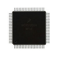
MC9S12D64MFUE Freescale, MC9S12D64MFUE Datasheet - Page 89

MC9S12D64MFUE
Manufacturer Part Number
MC9S12D64MFUE
Description
Manufacturer
Freescale
Datasheet
1.MC9S12D64MFUE.pdf
(128 pages)
Specifications of MC9S12D64MFUE
Cpu Family
HCS12
Device Core Size
16b
Frequency (max)
25MHz
Interface Type
CAN/I2C/SCI/SPI
Total Internal Ram Size
4KB
# I/os (max)
49
Number Of Timers - General Purpose
8
Operating Supply Voltage (typ)
2.5/5V
Operating Supply Voltage (max)
2.75/5.25V
Operating Supply Voltage (min)
2.35/4.5V
On-chip Adc
2(8-chx10-bit)
Instruction Set Architecture
CISC
Operating Temp Range
-40C to 125C
Operating Temperature Classification
Automotive
Mounting
Surface Mount
Pin Count
80
Package Type
PQFP
Program Memory Type
Flash
Program Memory Size
64KB
Lead Free Status / RoHS Status
Compliant
Available stocks
Company
Part Number
Manufacturer
Quantity
Price
Company:
Part Number:
MC9S12D64MFUE
Manufacturer:
Freescale Semiconductor
Quantity:
10 000
A.1.5 Absolute Maximum Ratings
Absolute maximum ratings are stress ratings only. A functional operation under or outside those maxima
is not guaranteed. Stress beyond those limits may affect the reliability or cause permanent damage of the
device.
This device contains circuitry protecting against damage due to high static voltage or electrical fields;
however, it is advised that normal precautions be taken to avoid application of any voltages higher than
maximum-rated voltages to this high-impedance circuit. Reliability of operation is enhanced if unused
inputs are tied to an appropriate logic voltage level (e.g., either V
NOTES:
Num
1. Beyond absolute maximum ratings device might be damaged.
2. The device contains an internal voltage regulator to generate the logic and PLL supply out of the I/O supply.
3. All digital I/O pins are internally clamped to V
4. Those pins are internally clamped to V
5. This pin is clamped low to V
10
11
12
13
1
2
3
4
5
6
7
8
9
The absolute maximum ratings apply when the device is powered from an external source.
I/O, Regulator and Analog Supply Voltage
Digital Logic Supply Voltage
PLL Supply Voltage
Voltage difference VDDX to VDDR and VDDA
Voltage difference VSSX to VSSR and VSSA
Digital I/O Input Voltage
Analog Reference
XFC, EXTAL, XTAL inputs
TEST input
Instantaneous Maximum Current
Single pin limit for all digital I/O pins
Instantaneous Maximum Current
Single pin limit for XFC, EXTAL, XTAL
Instantaneous Maximum Current
Single pin limit for TEST
Storage Temperature Range
Table A-1 Absolute Maximum Ratings
2
Rating
SSR
5
, but not clamped high. This pin must be tied low in applications.
2
SSPLL
3
4
and V
SSX
and V
DDPLL
DDX
.
, V
Symbol
V
SSR
V
V
RH,
V
V
DDPLL
VDDX
V
T
VSSX
V
TEST
I
I
DD5
MC9S12DJ64 Device User Guide — V01.20
I
DT
DL
DD
ILV
stg
D
IN
and V
V
SS5
RL
DDR
or V
or V
-0.25
Min
– 65
-0.3
-0.3
-0.3
-0.3
-0.3
-0.3
-0.3
-0.3
-0.3
DD5
-25
-25
1
SSA
).
and V
Max
DDA
10.0
+25
+25
155
6.0
3.0
3.0
0.3
0.3
6.0
6.0
3.0
0
.
Unit
mA
mA
mA
V
V
V
V
V
V
V
V
V
C
89


