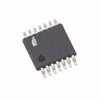
X9119TV14 Intersil, X9119TV14 Datasheet

X9119TV14
Specifications of X9119TV14
Available stocks
Related parts for X9119TV14
X9119TV14 Summary of contents
Page 1
... CAUTION: These devices are sensitive to electrostatic discharge; follow proper IC Handling Procedures. 1-888-INTERSIL or 1-888-468-3774 X9119 July 9, 2008 FN8162 100kΩ 1024-TAPS POT WIPER Intersil (and design registered trademark of Intersil Americas Inc. Copyright Intersil Americas Inc. 2005, 2008. All Rights Reserved All other trademarks mentioned are the property of their respective owners ...
Page 2
... X9119TV14Z-2.7* (Note) X9119 TVZF X9119TV14I-2.7 X9119 TVG X9119TV14IZ-2.7* (Note) X9119 TVZG *Add "T1" suffix for tape and reel. Please refer to TB347 for details on reel specifications. NOTE: These Intersil Pb-free plastic packaged products employ special Pb-free material sets, molding compounds/die attach materials, and 100% matte tin plate plus anneal (e3 termination finish, which is RoHS compliant and compatible with both SnPb and Pb-free soldering operations) ...
Page 3
Applications Circuit Level • Vary the gain of a voltage amplifier • Provide programmable DC reference voltages for comparators and detectors • Control the volume in audio circuits • Trim out the offset voltage error in a voltage amplifier circuit ...
Page 4
... Other Pins NO CONNECT No connect pins should be left open. These pins are used for Intersil manufacturing and testing purposes. Principals of Operation The X9119 is an integrated microcircuit incorporating a resistor array and its associated registers and counters and the serial interface logic providing direct communication between the host and the digitally controlled potentiometer ...
Page 5
STOP CONDITION All communications must be terminated by a stop condition, which is a LOW to HIGH transition of SDA while SCL is HIGH (see Figure 3). ACKNOWLEDGE Acknowledge is a software convention used to provide a positive handshake between ...
Page 6
Instruction and Register Description Device Addressing: Identification Byte (ID and A) Following a start condition, the master must output the address of the slave it is accessing. The most significant four bits of the slave address are the device type ...
Page 7
Instruction and Register Description Device Addressing WIPER COUNTER REGISTER (WCR) The X9119 contains a Wiper Counter Registers (refer to Table 4) for the XDCP potentiometer. The WCR is equivalent to a serial-in, parallel-out register/counter with its outputs decoded to select ...
Page 8
SCL SDA ID3 ID2 ID1 ID0 T A DEVICE SCL SDA ID3 ID2 ID1 ID0 R DEVICE ID INTERNAL ...
Page 9
WRITE DATA REGISTER (DR) DEVICE TYPE DEVICE INSTRUCTION IDENTIFIER ADDRESSES TRANSFER WIPER COUNTER REGISTER (WCR) TO DATA REGISTER (DR) DEVICE TYPE DEVICE S ...
Page 10
... W 10 X9119 Thermal Information Temperature under bias .-65°C to +135°C Storage temperature . . . . . . . . . . . . . . . . . . . . . . . .-65°C to +150°C Lead temperature (soldering, 10s 300°C Pb-Free Reflow Profile .see link below http://www.intersil.com/pbfree/Pb-FreeReflow.asp SYMBOL TEST CONDITIONS R TOTAL +25°C, each pot I W Wiper Current = ± 50µA, ...
Page 11
Operating Specifications (Over the recommended operating conditions unless otherwise specified.) PARAMETER SYMBOL V supply current I CC CC1 (active) V supply current I CC CC2 (nonvolatile write) V current (standby Input leakage current I LI Output leakage ...
Page 12
Equivalent A.C. Load Circuit 5V 1533Ω SDA OUTPUT 100pF AC Timing High-Voltage Write Cycle Timing PARAMETER Clock Frequency Clock Cycle Time Clock High Time Clock Low Time Start Setup Time Start Hold Time Stop Setup Time SDA Data Input Setup ...
Page 13
Symbol Table WAVEFORM INPUTS Must be steady May change from Low to High May change from High to Low Don’t Care: Changes Allowed N/A Timing Diagrams Start and Stop Timing ( START) SCL t SU:STA SDA Input Timing t CYC ...
Page 14
XDCP Timing (for All Load Instructions) SCL SDA R W Write Protect and Device Address Pins Timing SCL SDA WP A0, A1 X9119 LSB t WRL (START) (STOP) ... (ANY INSTRUCTION) ... ... T T SU:WPA HD:WPA (STOP) ...
Page 15
Applications information Basic Configurations of Electronic Potentiometers V R THREE TERMINAL POTENTIOMETER; VARIABLE VOLTAGE DIVIDER Application Circuits NONINVERTING AMPLIFIER – (1 OFFSET VOLTAGE ADJUSTMENT R 1 ...
Page 16
Application Circuits (Continued) ATTENUATOR – -1/2 £ G £ +1/2 INVERTING AMPLIFIER ...
Page 17
... Accordingly, the reader is cautioned to verify that data sheets are current before placing orders. Information furnished by Intersil is believed to be accurate and reliable. However, no responsibility is assumed by Intersil or its subsidiaries for its use; nor for any infringements of patents or other rights of third parties which may result from its use ...


