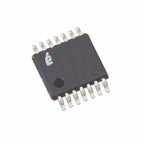
X9119TV14 Intersil, X9119TV14 Datasheet - Page 7

X9119TV14
Manufacturer Part Number
X9119TV14
Description
IC DCP 100K 1024TP 14TSSOP
Manufacturer
Intersil
Series
XDCP™r
Datasheet
1.X9119TV14.pdf
(17 pages)
Specifications of X9119TV14
Taps
1024
Resistance (ohms)
100K
Number Of Circuits
1
Temperature Coefficient
300 ppm/°C Typical
Memory Type
Non-Volatile
Interface
I²C, 2-Wire Serial
Voltage - Supply
4.5 V ~ 5.5 V
Operating Temperature
0°C ~ 70°C
Mounting Type
Surface Mount
Package / Case
14-TSSOP
Resistance In Ohms
100K
Lead Free Status / RoHS Status
Contains lead / RoHS non-compliant
Available stocks
Company
Part Number
Manufacturer
Quantity
Price
Company:
Part Number:
X9119TV14IZ-2.7
Manufacturer:
Intersil
Quantity:
254
Company:
Part Number:
X9119TV14IZ-2.7T1
Manufacturer:
DIODES
Quantity:
1 000
Company:
Part Number:
X9119TV14Z
Manufacturer:
Intersil
Quantity:
17
Instruction and Register Description
Device Addressing
WIPER COUNTER REGISTER (WCR)
The X9119 contains a Wiper Counter Registers (refer to
Table 4) for the XDCP potentiometer. The WCR is equivalent
to a serial-in, parallel-out register/counter with its outputs
decoded to select one of 1024 switches along its resistor
array. The contents of the WCR can be altered in one of
three ways:
The Wiper Counter Register is a volatile register; that is, its
contents are lost when the X9119 is powered-down.
Four of the six instructions are four bytes in length. These
instructions are:
• Read Wiper Counter Register – read the current wiper
• Write Wiper Counter Register – change current wiper
• Read Data Register – read the contents of the selected
• Write Data Register – write a new value to the selected
The basic sequence of the four byte instructions is illustrated
in Figure 3. These four-byte instructions exchange data
between the WCR and one of the Data Registers. A transfer
from a data register to a WCR is essentially a write to a static
RAM, with the static RAM controlling the wiper position. The
response of the wiper to this action will be delayed by t
A transfer from the WCR (current wiper position), to a data
register is a write-to-nonvolatile memory and takes a
minimum of t
between one of the four potentiometers and one of its
associated registers.
1. it may be written directly by the host via the write wiper
2. it may be written indirectly by transferring the contents of
3. it is loaded with the contents of its data register zero (R0)
position of the selected potentiometer,
position of the selected potentiometer,
Data Register;
Data Register.
TABLE 4. WIPER CONTROL REGISTER, WCR (10-BIT), WCR9–WCR0: Used to store the current wiper position (Volatile, V)
TABLE 5. DATA REGISTER, DR (10-BIT), BIT 9–BIT 0: Used to store wiper positions or data (Non-Volatile, NV)
WCR9
(MSB)
counter register instruction (serial load)
one of four associated data registers via the XFR data
register
upon power-up.
Bit 9
MSB
NV
V
WR
WCR8
Bit 8
to complete. The transfer can occur
NV
V
WCR7
Bit 7
7
NV
V
WCR6
Bit 6
NV
V
WCR5
WRL
Bit 5
NV
V
.
X9119
WCR4
Bit 4
NV
V
Although the register is automatically loaded with the value
in DR0 upon power-up, this may be different from the value
present at power-down. Power-up guidelines are
recommended to ensure proper loadings of the DR0 value
into the WCR.
DATA REGISTERS (DR0 TO DR3)
The potentiometer has four 10-bit non-volatile Data
Registers. These can be read or written directly by the host.
Data can also be transferred between any of the four Data
Registers and the Wiper Counter Register. All operations
changing data in one of the data registers is a nonvolatile
operation and will take a maximum of 10ms.
If the application does not require storage of multiple
settings for the potentiometer, the Data Registers can be
used as regular memory locations for system parameters or
user preference data.
Bit 9–Bit 0 are used to store one of the 1024 wiper position
(0 ~1023).
Two instructions (Figure 4) require a two-byte sequence to
complete. These instructions transfer data between the host
and the X9119; either between the host and one of the data
registers or directly between the host and the Wiper Counter
Register. These instructions are:
• XFR Data Register to Wiper Counter Register – This
• XFR Wiper Counter Register to Data Register – This
See “Instruction Format” on page 8 for more details.
POWER-UP AND DOWN REQUIREMENTS
There are no restrictions on the power-up condition of V
and the voltages applied to the potentiometer pins provided
that the V
voltages at R
are no restrictions on the power-down condition. However,
the datasheet parameters for the DCP do not apply until 1ms
after V
transfers the contents of one specified Data Register to
the Wiper Counter Register.
transfers the contents of the Wiper Counter Register to the
specified Data Register.
CC
WCR3
CC
reaches its final value.
Bit 3
NV
V
H
is always more positive than or equal to the
, R
L
, and R
WCR2
Bit 2
NV
V
W
, i.e. V
CC
WCR1
Bit 1
NV
V
≥ R
H
, R
L
, R
WCR0
(LSB)
Bit 0
LSB
W
NV
V
. There
July 9, 2008
FN8162.4
CC


