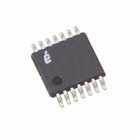
X9119TV14 Intersil, X9119TV14 Datasheet - Page 4

X9119TV14
Manufacturer Part Number
X9119TV14
Description
IC DCP 100K 1024TP 14TSSOP
Manufacturer
Intersil
Series
XDCP™r
Datasheet
1.X9119TV14.pdf
(17 pages)
Specifications of X9119TV14
Taps
1024
Resistance (ohms)
100K
Number Of Circuits
1
Temperature Coefficient
300 ppm/°C Typical
Memory Type
Non-Volatile
Interface
I²C, 2-Wire Serial
Voltage - Supply
4.5 V ~ 5.5 V
Operating Temperature
0°C ~ 70°C
Mounting Type
Surface Mount
Package / Case
14-TSSOP
Resistance In Ohms
100K
Lead Free Status / RoHS Status
Contains lead / RoHS non-compliant
Available stocks
Company
Part Number
Manufacturer
Quantity
Price
Company:
Part Number:
X9119TV14IZ-2.7
Manufacturer:
Intersil
Quantity:
254
Company:
Part Number:
X9119TV14IZ-2.7T1
Manufacturer:
DIODES
Quantity:
1 000
Company:
Part Number:
X9119TV14Z
Manufacturer:
Intersil
Quantity:
17
R
The wiper pin are equivalent to the wiper terminal of a
mechanical potentiometer.
Bias Supply Pins
SYSTEM SUPPLY VOLTAGE (V
GROUND (V
The V
the system ground.
Other Pins
NO CONNECT
No connect pins should be left open. These pins are used for
Intersil manufacturing and testing purposes.
Principals of Operation
The X9119 is an integrated microcircuit incorporating a
resistor array and its associated registers and counters and
the serial interface logic providing direct communication
between the host and the digitally controlled potentiometer.
This section provides detail description of the following:
• Resistor Array Description
• Serial Interface Description
• Instruction and Register Description
Resistor Array Description
The X9119 is comprised of a resistor array. The array
contains, in effect, 1023 discrete resistive segments that are
connected in series (Figure 1). The physical ends of each
array are equivalent to the fixed terminals of a mechanical
potentiometer (R
W
IF WCR = 000[HEX] THEN R
IF WCR = 3FF[HEX] THEN R
CC
FROM INTERFACE
SERIAL DATA PATH
CIRCUITRY
pin is the system supply voltage. The V
SS
)
H
and R
FIGURE 1. DETAILED POTENTIOMETER BLOCK DIAGRAM SERIAL INTERFACE DESCRIPTION
L
W
W
inputs).
= R
= R
4
L
H
REGISTER 0
REGISTER 2
CC
(DR0)
(DR2)
) AND SUPPLY
10
SS
pin is
REGISTER 1
REGISTER 3
(DR1)
(DR3)
X9119
10
At both ends of each array and between each resistor
segment is a CMOS switch connected to the wiper (R
output. Within each individual array only one switch may be
turned on at a time. These switches are controlled by the
Wiper Counter Register (WCR). The 10-bits of the WCR
(WCR[9:0]) are decoded to select, and enable, one of 1024
switches.
The WCR may be written directly. The Data Registers and
the WCR can be read and written by the host system.
Serial Interface Description
SERIAL INTERFACE
The X9119 supports a bidirectional bus oriented protocol.
The protocol defines any device that sends data onto the
bus as a transmitter and the receiving device as the receiver.
The device controlling the transfer is a master and the
device being controlled is the slave. The master will always
initiate data transfers and provide the clock for both transmit
and receive operations. Therefore, the X9119 will be
considered a slave device in all applications.
CLOCK AND DATA CONVENTIONS
Data states on the SDA line can change only during SCL
LOW periods. SDA state changes during SCL HIGH are
reserved for indicating start and stop conditions (Figure 3).
START CONDITION
All commands to the X9119 are preceded by the start
condition, which is a HIGH to LOW transition of SDA while
SCL is HIGH. The X9119 continuously monitors the SDA
and SCL lines for the start condition and will not respond to
any command until this condition is met (Figure 3).
BUS
INPUT
SERIAL
BUS
INPUT
PARALLEL
REGISTER
COUNTER
WIPER
(WCR)
C
O
U
N
T
E
R
D
E
C
O
D
E
R
R H
R L
R
W
July 9, 2008
W
FN8162.4
)


