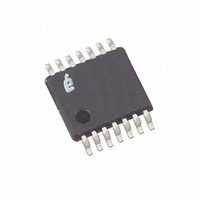
X9119TV14 Intersil, X9119TV14 Datasheet - Page 6

X9119TV14
Manufacturer Part Number
X9119TV14
Description
IC DCP 100K 1024TP 14TSSOP
Manufacturer
Intersil
Series
XDCP™r
Datasheet
1.X9119TV14.pdf
(17 pages)
Specifications of X9119TV14
Taps
1024
Resistance (ohms)
100K
Number Of Circuits
1
Temperature Coefficient
300 ppm/°C Typical
Memory Type
Non-Volatile
Interface
I²C, 2-Wire Serial
Voltage - Supply
4.5 V ~ 5.5 V
Operating Temperature
0°C ~ 70°C
Mounting Type
Surface Mount
Package / Case
14-TSSOP
Resistance In Ohms
100K
Lead Free Status / RoHS Status
Contains lead / RoHS non-compliant
Available stocks
Company
Part Number
Manufacturer
Quantity
Price
Company:
Part Number:
X9119TV14IZ-2.7
Manufacturer:
Intersil
Quantity:
254
Company:
Part Number:
X9119TV14IZ-2.7T1
Manufacturer:
DIODES
Quantity:
1 000
Company:
Part Number:
X9119TV14Z
Manufacturer:
Intersil
Quantity:
17
Instruction and Register Description
Device Addressing: Identification Byte (ID and A)
Following a start condition, the master must output the
address of the slave it is accessing. The most significant four
bits of the slave address are the device type identifier. The
ID[3:0] bits is the device id for the X9119; this is fixed as
0101[B] (refer to Table 1).
The A2–A0 bits in the ID byte is the internal slave address.
The physical device address is defined by the state of the
A2–A0 input pins. The slave address is externally specified
by the user. The X9119 compares the serial data stream with
the address input state; a successful compare of both
address bits is required for the X9119 to successfully
continue the command sequence. Only the device which
NOTE: 1/0 = data is one or zero.
Read Wiper Counter
Register
Write Wiper Counter
Register
Read Data Register
Write Data Register
XFR Data Register to
Wiper Counter Register
XFR Wiper Counter Register
to Data Register
TABLE 1. IDENTIFICATION BYTE FORMAT
TABLE 2. INSTRUCTION BYTE FORMAT
TABLE 3. INSTRUCTION SET
REGISTER SELECTED
(MSB)
(MSB)
ID3
INSTRUCTION
I2
0
DR0
DR1
DR2
DR3
INSTRUCTION
OPCODE
ID2
I1
1
DEVICE TYPE
IDENTIFIES
R/W
1
0
1
0
1
0
6
RB
0
0
1
1
I
1
1
1
1
1
1
2
ID1
I0
0
I
0
0
0
1
1
1
1
I
0
1
1
0
0
1
0
INSTRUCTION SET
RA
0
1
0
1
ID0
0
0
0
0
0
0
0
1
0
RB
1/0
1/0
1/0
1/0
0
0
X9119
RA
1/0
1/0
1/0
1/0
0
0
slave address matches the incoming device address sent by
the master executes the instruction. The A2–A0 inputs can
be actively driven by CMOS input signals or tied to V
V
device for read or write operations.
INSTRUCTION BYTE AND REGISTER SELECTION
The next byte sent to the X9119 contains the instruction and
register pointer information. The three most significant bits
are used provide the instruction opcode (IOP[2:0]). The RB
and RA bits point to one of the four registers. The format is
shown below in Table 2.
Table 3 provides a complete summary of the instruction set
opcodes.
RB
A2
SS
0
0
0
0
0
0
0
. The R/W bit is the LSB and is be used to program the
SELECTION
REGISTER
0
0
0
0
0
0
0
INTERNAL SLAVE
Read the contents of the Wiper Counter
Register
Write new value to the Wiper Counter
Register
Read the contents of the Data Register pointed to
RB-RA.
Write new value to the Data Register
pointed to RB-RA.
Transfer the contents of the Data Register
pointed to by RB-RA.to the Wiper Counter
Register
Transfer the contents of the Wiper Counter
Register to the Data Register pointed to by
RB-RA.
ADDRESS
RA
A1
OPERATION
A0
0
WRITE BIT
READ OR
(LSB)
(LSB)
R/W
0
July 9, 2008
CC
FN8162.4
or


