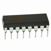
DAC8143FP Analog Devices Inc, DAC8143FP Datasheet - Page 10

DAC8143FP
Manufacturer Part Number
DAC8143FP
Description
IC DAC 12BIT DAISY-CHAIN 16-DIP
Manufacturer
Analog Devices Inc
Datasheet
1.DAC8143FSZ.pdf
(12 pages)
Specifications of DAC8143FP
Rohs Status
RoHS non-compliant
Settling Time
380ns
Number Of Bits
12
Data Interface
Serial
Number Of Converters
1
Voltage Supply Source
Single Supply
Power Dissipation (max)
500µW
Operating Temperature
-40°C ~ 85°C
Mounting Type
Through Hole
Package / Case
16-DIP (0.300", 7.62mm)
Number Of Channels
1
Resolution
12b
Interface Type
Serial (3-Wire)
Single Supply Voltage (typ)
5V
Dual Supply Voltage (typ)
Not RequiredV
Architecture
R-2R
Power Supply Requirement
Single
Output Type
Current
Integral Nonlinearity Error
±1LSB
Single Supply Voltage (min)
4.75V
Single Supply Voltage (max)
5.25V
Dual Supply Voltage (min)
Not RequiredV
Dual Supply Voltage (max)
Not RequiredV
Operating Temp Range
-40C to 85C
Operating Temperature Classification
Industrial
Mounting
Through Hole
Pin Count
16
Package Type
PDIP
Lead Free Status / Rohs Status
Not Compliant
Available stocks
Company
Part Number
Manufacturer
Quantity
Price
Part Number:
DAC8143FPZ
Manufacturer:
ADI/亚德诺
Quantity:
20 000
In many applications, the DAC8143’s zero scale error and low
gain error, permit the elimination of external trimming compo-
nents without adverse effects on circuit performance.
For applications requiring a tighter gain error than 0.024% at
25 C for the top grade part, or 0.048% for the lower grade part,
the circuit in Figure 17 may be used. Gain error may be trimmed
by adjusting R1.
The DAC register must first be loaded with all 1s. R1 is then
adjusted until V
adjustable V
adjusted to yield the desired full-scale output.
BIPOLAR OPERATION (4-QUADRANT)
Figure 18 details a suggested circuit for bipolar, or offset binary,
operation. Table III shows the digital input-to-analog output
relationship. The circuit uses offset binary coding. Twos comple-
ment code can be converted to offset binary by software inver-
sion of the MSB or by the addition of an external inverter to the
MSB input.
Resistor R3, R4 and R5 must be selected to match within 0.01%
and must all be of the same (preferably metal foil) type to assure
temperature coefficient match. Mismatching between R3 and
R4 causes offset and full-scale error.
Calibration is performed by loading the DAC register with
1000 0000 0000 and adjusting R1 until V
R2 may be omitted by adjusting the ratio of R3 to R4 to yield
V
register with 1111 1111 1111 and adjusting either the amplitude
of V
DAC8143
OUT
REF
= 0 V. Full scale can be adjusted by loading the DAC
or the value of R5 until the desired V
REF
V
, R1 and R
DATA INPUT
IN
OUT
SERIAL
= –V
REF
100
FEEDBACK
R1
(4095/4096). In the case of an
12
15
7
8-11
DGND
V
SRI
REF
CONTROL
CONTROL
may be omitted, with V
Figure 18. Bipolar Operation (4-Quadrant, Offset Binary)
INPUTS
BITS
4, 5
DAC8143
OUT
+5V
V
SYSTEM
DD
RESET
FROM
14
OUT
CLR
= 0 V. R1 and
13
is achieved.
SRO
R
6
FB
15
AGND
BUFFERED SERIAL
DATA OUT
I
I
OUT1
OUT2
50
REF
R2
1
3
COMMON GROUND
2
–10–
C1
10-33pF
Digital Input
MSB
1 1 1 1 1 1 1 1 1 1 1 1
1 0 0 0 0 0 0 0 0 0 0 1
1 0 0 0 0 0 0 0 0 0 0 0
0 1 1 1 1 1 1 1 1 1 1 1
0 0 0 0 0 0 0 0 0 0 0 1
0 0 0 0 0 0 0 0 0 0 0 0
NOTES
1
2
DAISY-CHAINING DAC8143s
Many applications use multiple serial input DACs that use
numerous interconnecting lines for address decoding and data
lines. In addition, they use some type of buffering to reduce
loading on the bus. The DAC8143 is ideal for just such an
application. It not only reduces the number of interconnecting
lines, but also reduces bus loading. The DAC8143 can be daisy-
chained with only three lines: one data line, one CLK line and
one load line, see Figure 19.
Nominal full scale for the circuits of Figure 18 is given by
FS = V
Nominal LSB magnitude for the circuits of Figure 18 is given by
LSB = V
1/2 OP200
REF
A1
REF
Table III. Bipolar (Offset Binary) Code Table
2047
2048
2048
1
.
.
10k
LSB
R3
R4
20k
1/2 OP200
Nominal Analog Output
(V
+V
+V
0
–V
–V
–V
A2
OUT
REF
REF
REF
REF
REF
20k
R5
as Shown in Figure 18)
2048
2047
2048
2048
2048
2047
2048
2048
1
1
V
OUT
REV. C


