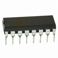
DAC8143FP Analog Devices Inc, DAC8143FP Datasheet - Page 8

DAC8143FP
Manufacturer Part Number
DAC8143FP
Description
IC DAC 12BIT DAISY-CHAIN 16-DIP
Manufacturer
Analog Devices Inc
Datasheet
1.DAC8143FSZ.pdf
(12 pages)
Specifications of DAC8143FP
Rohs Status
RoHS non-compliant
Settling Time
380ns
Number Of Bits
12
Data Interface
Serial
Number Of Converters
1
Voltage Supply Source
Single Supply
Power Dissipation (max)
500µW
Operating Temperature
-40°C ~ 85°C
Mounting Type
Through Hole
Package / Case
16-DIP (0.300", 7.62mm)
Number Of Channels
1
Resolution
12b
Interface Type
Serial (3-Wire)
Single Supply Voltage (typ)
5V
Dual Supply Voltage (typ)
Not RequiredV
Architecture
R-2R
Power Supply Requirement
Single
Output Type
Current
Integral Nonlinearity Error
±1LSB
Single Supply Voltage (min)
4.75V
Single Supply Voltage (max)
5.25V
Dual Supply Voltage (min)
Not RequiredV
Dual Supply Voltage (max)
Not RequiredV
Operating Temp Range
-40C to 85C
Operating Temperature Classification
Industrial
Mounting
Through Hole
Pin Count
16
Package Type
PDIP
Lead Free Status / Rohs Status
Not Compliant
Available stocks
Company
Part Number
Manufacturer
Quantity
Price
Part Number:
DAC8143FPZ
Manufacturer:
ADI/亚德诺
Quantity:
20 000
DAC8143
Where R
Therefore, the offset gain varies as follows:
at code 0011 1111 1111,
at code 0100 0000 0000,
The error difference is 2/3 V
Since one LSB has a weight (for V
the DAC8143, it is clearly important that V
using either the amplifier’s pulling pins, an external pulling
network, or by selection of an amplifier with inherently low V
Amplifiers with sufficiently low V
OP27, and OP42.
INTERFACE LOGIC OPERATION
The microprocessor interface of the DAC8143 has been design-
ed with multiple STROBE and LOAD inputs to maximize inter-
facing options. Control signals decoding may be done on chip or
with the use of external decoding circuitry (see Figure 21).
Serial data is clocked into the input register and buffered output
stage with STB
on the rising edge. STB3 may be used with a falling edge clock
data.
R
R
O
O
= 10 k for more than four bits of Logic 1,
= 30 k for any single bit of Logic 1.
O
is a function of the digital code, and:
V
V
1
ERROR2
, STB
ERROR1
(STB
1
2
, STB
LD
= V
, or STB
= V
*
1
t
STROBE
AND LD
DS1
2
, STB
OS
,
OS
SRO
t
SRI
DS2
OS
4
2
)
,
1
.
t
1
DS3
OS
4
NOTES:
*
**
. The strobe inputs are active
STROBE WAVEFORM IS INVERTED IF
BITS INTO INPUT REGISTER.
THE INPUT SHIFT REGISTER MSB FIRST.
STB
DATA IS STROBED INTO AND OUT OF
10 k
30 k
,
10 k
10 k
t
REF
include OP77, OP97, OP07,
DS4
3
IS USED TO STROBE SERIAL DATA
BIT 1
MSB
t
t
t
t
STB1
STB2
STB3
STB4
= +10 V) of 2.4 mV for
= 4/3 V
BIT 1
MSB
= 2 V
LOAD NEW 12-BIT WORD INTO
t
INPUT REGISTER AND SHIFT
PD
1
OS
OUT PREVIOUS WORD
WORD N –2
be minimized,
BIT 2
OS
OS
BIT 2
t
DH1
t
t
t
t
2
STB1
STB2
STB3
STB4
,
Figure 15. Timing Diagram
t
DH2
WORD N –1
,
t
DH3
,
t
DH4
12
OS
t
ASB
.
–8–
BIT 12
BIT 1
LSB
MSB
Serial data output (SRO) follows the serial data input (SRI) by
12 clocked bits.
Holding any STROBE input at its selected state (i.e., STB
STB
prevent any further data input.
When a new data word has been entered into the input register,
it is transferred to the DAC register by asserting both LOAD
inputs.
The CLR input allows asynchronous resetting of the DAC regis-
ter to 0000 0000 0000. This reset does not affect data held in
the input registers. While in unipolar mode, a CLEAR will
result in the analog output going to 0 V. In bipolar mode, the
output will go to –V
INTERFACE INPUT DESCRIPTION
STB
and Buffered Output Strobe. Inputs Active on Rising
Edge. Selected to load serial data into input register and buff-
ered output stage. See Table I for details.
STB3 (Pin 10)—Input Register and Buffered Output
Strobe Input. Active on Falling Edge. Selected to load serial
data into input register and buffered output stage. See Table I
for details.
LD1 (Pin 5), LD2 (Pin 9)—Load DAC Register Inputs.
Active Low. Selected together to load contents of input register
into DAC register.
CLR (Pin 13)—Clear Input. Active Low. Asynchronous.
When LOW, 12-bit DAC register is forced to a zero code (0000
0000 0000) regardless of other interface inputs.
LOAD INPUT REGISTER'S
DATA INTO DAC REGISTER
t
t
LD1
LD2
2
1
1
or STB
(Pin 4), STB
BIT 1
MSB
BIT 2
t
SR1
2
WORD N –1
4
at logic HIGH or STB
BIT 2
REF
2
(Pin 8), STB
.
WORD N
11
BIT 12
LSB
BIT 11
4
12
(Pin 11)—Input Register
3
at logic LOW) will act to
WORD N
BIT 1
LSB
BIT 12
LSB
REV. C
1
,


