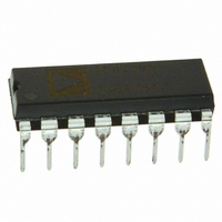
DAC8143FP Analog Devices Inc, DAC8143FP Datasheet - Page 9

DAC8143FP
Manufacturer Part Number
DAC8143FP
Description
IC DAC 12BIT DAISY-CHAIN 16-DIP
Manufacturer
Analog Devices Inc
Datasheet
1.DAC8143FSZ.pdf
(12 pages)
Specifications of DAC8143FP
Rohs Status
RoHS non-compliant
Settling Time
380ns
Number Of Bits
12
Data Interface
Serial
Number Of Converters
1
Voltage Supply Source
Single Supply
Power Dissipation (max)
500µW
Operating Temperature
-40°C ~ 85°C
Mounting Type
Through Hole
Package / Case
16-DIP (0.300", 7.62mm)
Number Of Channels
1
Resolution
12b
Interface Type
Serial (3-Wire)
Single Supply Voltage (typ)
5V
Dual Supply Voltage (typ)
Not RequiredV
Architecture
R-2R
Power Supply Requirement
Single
Output Type
Current
Integral Nonlinearity Error
±1LSB
Single Supply Voltage (min)
4.75V
Single Supply Voltage (max)
5.25V
Dual Supply Voltage (min)
Not RequiredV
Dual Supply Voltage (max)
Not RequiredV
Operating Temp Range
-40C to 85C
Operating Temperature Classification
Industrial
Mounting
Through Hole
Pin Count
16
Package Type
PDIP
Lead Free Status / Rohs Status
Not Compliant
Available stocks
Company
Part Number
Manufacturer
Quantity
Price
Part Number:
DAC8143FPZ
Manufacturer:
ADI/亚德诺
Quantity:
20 000
DAC8143 Logic Inputs
Input Register/
Digital Output
STB
0
0
0
g
1
X
X
X
NOTES
1
2
3
REV. C
APPLICATIONS INFORMATION
UNIPOLAR OPERATION (2-QUADRANT)
The circuit shown in Figures 16 and 17 may be used with an ac
or dc reference voltage. The circuit’s output will range between
0 V and +10(4095/4096) V depending upon the digital input
code. The relationship between the digital input and the analog
output is shown in Table II. The V
mum input voltage range of the op amp or 25 V, whichever is
lowest.
Digital Input
MSB
1 1 1 1 1 1 1 1 1 1 1 1
1 0 0 0 0 0 0 0 0 0 0 1
1 0 0 0 0 0 0 0 0 0 0 0
0 1 1 1 1 1 1 1 1 1 1 1
0 0 0 0 0 0 0 0 0 0 0 1
0 0 0 0 0 0 0 0 0 0 0 0
NOTES
1
2
CLR = 0 asynchronously resets DAC Register to 0000 0000 0000, but has no effect on Input Register.
Serial data is loaded into Input Register MSB first, on edges shown. g is positive edge, f is negative edge.
0 = Logic LOW, 1 = Logic HIGH, X = Don’t Care.
Nominal full scale for the circuits of Figures 16 and 17 is given by
FS = –V
Nominal LSB magnitude for the circuits of Figures 16 and 17 is given by
LSB = V
4
REF
REF
STB3
1
1
f
1
X
0
X
X
4096
4095
4096
1
Table II. Unipolar Code Table
.
LSB
or V
Control Inputs
STB
0
g
0
0
X
X
1
X
REF
(2
2
–n
).
STB
g
0
0
0
X
X
X
1
Nominal Analog Output
(V
in Figures 16 and 17)
–V
–V
–V
–V
–V
–V
REF
OUT
REF
REF
REF
REF
REF
REF
1
voltage range is the maxi-
as Shown
4095
4096
2047
4096
2049
4096
2048
4096
4096
4096
DAC Register
CLR
X
X
X
X
0
1
1
1
1
0
= –
= 0
V
REF
2
Table I. Truth Table
Control Inputs
LD2
X
X
X
X
X
1
X
0
–9–
Figure 16. Unipolar Operation with High Accuracy Op
Amp (2-Quadrant)
LD1
X
X
X
X
X
X
1
0
CONTROL
CONTROL
Figure 17. Unipolar Operation with Fast Op Amp and
Gain Error Trimming (2-Quadrant)
DATA IN)
DATA IN)
(SERIAL
(SERIAL
V
–10V
V
–10V
CLR
INPUTS
CLR
INPUTS
SRI
SRI
REF
REF
100
R1
V
DAC8143 Operation
Serial Data Bit Loaded from SRI
into Input Register and Digital Output
(SRO Pin) after 12 Clocked Bits.
No Operation (Input Register and SRO)
Reset DAC Register to Zero Code
(Code: 0000 0000 0000)
(Asynchronous Operation)
No Operation (DAC Register and SRO)
Load DAC Register with the Contents
of Input Register
REF
13
4, 5
8–11
7
13
4, 5
8–11
7
15
DAC8143
15
DAC8143
V
DGND
DGND
REF
12
12
V
DD
+5V
+5V
14
14
V
1
2
3
6
1
2
3
6
DD
R
R
I
I
AGND
SRO
(BUFFERED
DIGITAL
DATA OUT)
I
I
AGND
SRO
(BUFFERED
DIGITAL
DATA OUT)
OUT1
OUT2
OUT1
OUT2
FEEDBACK
FEEDBACK
50
R2
15pF
15pF
2
3
2
3
OP-42
OP-77
DAC8143
–15V
+15V
+15V
–15V
7
7
4
4
6
6
Notes
2, 3
3
1, 3
3
3
V
V
OUT
OUT


