DAC8143FP Analog Devices Inc, DAC8143FP Datasheet - Page 6
DAC8143FP
Manufacturer Part Number
DAC8143FP
Description
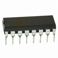
IC DAC 12BIT DAISY-CHAIN 16-DIP
Manufacturer
Analog Devices Inc
Datasheet
1.DAC8143FSZ.pdf
(12 pages)
Specifications of DAC8143FP
Rohs Status
RoHS non-compliant
Settling Time
380ns
Number Of Bits
12
Data Interface
Serial
Number Of Converters
1
Voltage Supply Source
Single Supply
Power Dissipation (max)
500µW
Operating Temperature
-40°C ~ 85°C
Mounting Type
Through Hole
Package / Case
16-DIP (0.300", 7.62mm)
Number Of Channels
1
Resolution
12b
Interface Type
Serial (3-Wire)
Single Supply Voltage (typ)
5V
Dual Supply Voltage (typ)
Not RequiredV
Architecture
R-2R
Power Supply Requirement
Single
Output Type
Current
Integral Nonlinearity Error
±1LSB
Single Supply Voltage (min)
4.75V
Single Supply Voltage (max)
5.25V
Dual Supply Voltage (min)
Not RequiredV
Dual Supply Voltage (max)
Not RequiredV
Operating Temp Range
-40C to 85C
Operating Temperature Classification
Industrial
Mounting
Through Hole
Pin Count
16
Package Type
PDIP
Lead Free Status / Rohs Status
Not Compliant
Available stocks
Company
Part Number
Manufacturer
Quantity
Price

Part Number:
DAC8143FPZ
Manufacturer:
ADI/亚德诺
Quantity:
20 000


DAC8143
DEFINITION OF SPECIFICATIONS
RESOLUTION
The resolution of a DAC is the number of states (2
the full-scale range (FSR) is divided (or resolved), where “n” is
equal to the number of bits.
SETTLING TIME
Time required for the analog output of the DAC to settle to
within 1/2 LSB of its final value for a given digital input stimu-
lus; i.e., zero to full-scale.
GAIN
Ratio of the DAC’s external operational amplifier output voltage
to the V
FEEDTHROUGH ERROR
Error caused by capacitive coupling from V
Feedthrough error limits are specified with all switches off.
OUTPUT CAPACITANCE
Capacitance from I
OUTPUT LEAKAGE CURRENT
Current appearing at I
at I
GENERAL CIRCUIT INFORMATION
The DAC8143 is a 12-bit serial-input, buffered serial-output,
multiplying CMOS D/A converter. It has an R-2R resistor lad-
der network, a 12-bit input shift register, 12-bit DAC register,
control logic circuitry, and a buffered digital output stage.
The control logic forms an interface in which serial data is
loaded, under microprocessor control, into the input shift regis-
ter and then transferred, in parallel, to the DAC register. In
addition, buffered serial output data is present at the SRO pin
when input data is loaded into the input register. This buffered
data follows the digital input data (SRI) by 12 clock cycles and
is available for daisy-chaining additional DACs.
An asynchronous CLEAR function allows resetting the DAC
register to a zero code (0000 0000 0000) without altering data
stored in the registers.
OUT2
REF
terminal when all inputs are HIGH.
input voltage when all digital inputs are HIGH.
OUT1
OUT1
to ground.
when all digital inputs are LOW, or
REF
to output.
n
) into which
–6–
A simplified circuit of the DAC8143 is shown in Figure 10. An
inversed R-2R ladder network consisting of silicon-chrome,
thin-film resistors, and twelve pairs of NMOS current-steering
switches. These switches steer binarily weighted currents into
either I
a constant current in each ladder leg, regardless of digital input
code. This constant current results in a constant input resis-
tance at V
be driven by any reference voltage or current, ac or dc, that is
within the limits stated in the Absolute Maximum Ratings chart.
The twelve output current-steering switches are in series with
the R-2R resistor ladder, and therefore, can introduce bit errors.
It was essential to design these switches such that the switch
“ON” resistance be binarily scaled so that the voltage drop
across each switch remains constant. If, for example, Switch 1
of Figure 10 was designed with an “ON” resistance of 10 ,
Switch 2 for 20 , etc., a constant 5 mV drop would then be
maintained across each switch.
To further ensure accuracy across the full temperature range,
permanently “ON” MOS switches were included in series with
the feedback resistor and the R-2R ladder’s terminating resistor.
The Simplified DAC Circuit, Figure 10, shows the location of
these switches. These series switches are equivalently scaled to
two times Switch 1 (MSB) and top Switch 12 (LSB) to main-
tain constant relative voltage drops with varying temperature.
During any testing of the resistor ladder or R
incoming inspection), V
series switches.
V
REF
(SWITCHES SHOWN FOR DIGITAL INPUTS "HIGH")
BIT 1 (MSB)
OUT1
20k
S
1
10k
REF
or I
Figure 10. Simplified DAC Circuit
equal to R (typically 11 k ). The V
BIT 2
OUT2
DIGITAL INPUTS
20k
S
10k
2
. Switching current to I
BIT 3
DD
20k
S
3
must be present to turn “ON” these
10k
BIT 12 (LSB)
S
20k
12
20k
*
OUT1
*
FEEDBACK
THESE SWITCHES
PERMANENTLY "ON"
*
or I
REF
10k
OUT2
input may
(such as
R
FEEDBACK
REV. C
I
I
OUT2
OUT1
yields
Related parts for DAC8143FP
Image
Part Number
Description
Manufacturer
Datasheet
Request
R

Part Number:
Description:
Manufacturer:
ON Semiconductor
Datasheet:

Part Number:
Description:
DAC (D/A Converters) IC DAC 4CH I2C ADJ justable Sink-Source
Manufacturer:
Maxim Integrated Products
Datasheet:
Part Number:
Description:
DAC (D/A Converters) IC DAC 2CH I2C ADJ justable Sink-Source
Manufacturer:
Maxim Integrated Products
Datasheet:

Part Number:
Description:
DAC (D/A Converters) 12-Bit Precision DAC
Manufacturer:
Maxim Integrated Products
Datasheet:
Part Number:
Description:
DAC (D/A Converters) 8-Bit Precision DAC
Manufacturer:
Maxim Integrated Products
Datasheet:
Part Number:
Description:
DAC (D/A Converters) 12-Bit Precision DAC
Manufacturer:
Maxim Integrated Products
Datasheet:
Part Number:
Description:
DAC (D/A Converters) 8-Bit Precision DAC
Manufacturer:
Maxim Integrated Products
Datasheet:
Part Number:
Description:
DAC (D/A Converters) 8-Bit Precision DAC
Manufacturer:
Maxim Integrated Products
Datasheet:
Part Number:
Description:
DAC (D/A Converters) 8-Bit 2Ch Precision DAC
Manufacturer:
Maxim Integrated Products
Datasheet:
Part Number:
Description:
DAC (D/A Converters) 8-Bit 2Ch Precision DAC
Manufacturer:
Maxim Integrated Products
Datasheet:
Part Number:
Description:
DAC (D/A Converters) 12-Bit 2Ch Precision DAC
Manufacturer:
Maxim Integrated Products
Datasheet:
Part Number:
Description:
DAC (D/A Converters) 8-Bit 2Ch Precision DAC
Manufacturer:
Maxim Integrated Products
Datasheet:
Part Number:
Description:
DAC (D/A Converters) 8-Bit 2Ch Precision DAC
Manufacturer:
Maxim Integrated Products
Datasheet:
Part Number:
Description:
DAC (D/A Converters) 12-Bit 2Ch Precision DAC
Manufacturer:
Maxim Integrated Products
Datasheet:
Part Number:
Description:
DAC (D/A Converters) 14-Bit Precision DAC
Manufacturer:
Maxim Integrated Products
Datasheet: