DAC8143FP Analog Devices Inc, DAC8143FP Datasheet - Page 4
DAC8143FP
Manufacturer Part Number
DAC8143FP
Description
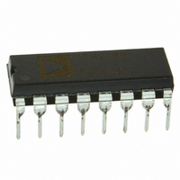
IC DAC 12BIT DAISY-CHAIN 16-DIP
Manufacturer
Analog Devices Inc
Datasheet
1.DAC8143FSZ.pdf
(12 pages)
Specifications of DAC8143FP
Rohs Status
RoHS non-compliant
Settling Time
380ns
Number Of Bits
12
Data Interface
Serial
Number Of Converters
1
Voltage Supply Source
Single Supply
Power Dissipation (max)
500µW
Operating Temperature
-40°C ~ 85°C
Mounting Type
Through Hole
Package / Case
16-DIP (0.300", 7.62mm)
Number Of Channels
1
Resolution
12b
Interface Type
Serial (3-Wire)
Single Supply Voltage (typ)
5V
Dual Supply Voltage (typ)
Not RequiredV
Architecture
R-2R
Power Supply Requirement
Single
Output Type
Current
Integral Nonlinearity Error
±1LSB
Single Supply Voltage (min)
4.75V
Single Supply Voltage (max)
5.25V
Dual Supply Voltage (min)
Not RequiredV
Dual Supply Voltage (max)
Not RequiredV
Operating Temp Range
-40C to 85C
Operating Temperature Classification
Industrial
Mounting
Through Hole
Pin Count
16
Package Type
PDIP
Lead Free Status / Rohs Status
Not Compliant
Available stocks
Company
Part Number
Manufacturer
Quantity
Price

Part Number:
DAC8143FPZ
Manufacturer:
ADI/亚德诺
Quantity:
20 000


ABSOLUTE MAXIMUM RATINGS
(T
V
V
V
AGND to DGND . . . . . . . . . . . . . . . . . . . . . . . . V
DGND to AGND . . . . . . . . . . . . . . . . . . . . . . . . V
Digital Input Voltage Range . . . . . . . . . . . . . . . –0.3 V to V
Output Voltage (Pin 1, Pin 2) . . . . . . . . . . . . . . –0.3 V to V
Operating Temperature Range
Junction Temperature . . . . . . . . . . . . . . . . . . . . . . . . . +150 C
Storage Temperature . . . . . . . . . . . . . . . . . . –65 C to +150 C
Lead Temperature (Soldering, 60 sec) . . . . . . . . . . . . +300 C
Package Type
16-Lead Plastic DIP
16-Lead SOIC
*
CAUTION
1. Do not apply voltage higher than V
2. The digital control inputs are Zener-protected; however,
3. Use proper antistatic handling procedures.
4. Absolute Maximum Ratings apply to packaged devices.
DAC8143
Model
DAC8143FP
DAC8143FS
Die Size: 99
CAUTION
ESD (electrostatic discharge) sensitive device. Electrostatic charges as high as 4000 V readily
accumulate on the human body and test equipment and can discharge without detection.
Although the DAC8143 features proprietary ESD protection circuitry, permanent damage may
occur on devices subjected to high energy electrostatic discharges. Therefore, proper ESD
precautions are recommended to avoid performance degradation or loss of functionality.
device in socket for P-DIP package;
printed circuit board for SOIC package.
DD
REF
RFB
JA
A
FP/FS Versions . . . . . . . . . . . . . . . . . . . . . –40 C to +85 C
tential on any terminal except V
permanent damage may occur on unprotected units from
high energy electrostatic fields. Keep units in conductive
foam at all times until ready to use.
Stresses above those listed under Absolute Maximum Ratings
may cause permanent damage to the device.
= +25 C, unless otherwise noted.)
is specified for worst case mounting conditions, i.e.,
to DGND . . . . . . . . . . . . . . . . . . . . . . . . . . . . . . . . +17 V
to DGND . . . . . . . . . . . . . . . . . . . . . . . . . . . . . . . 25 V
to DGND . . . . . . . . . . . . . . . . . . . . . . . . . . . . . . . 25 V
107 mil, 10,543 sq. mils.
Nonlinearity
1 LSB
1 LSB
JA
is specified for device soldered to
76
92
REF
JA
*
DD
(Pin 15) and R
or less than DGND po-
33
27
Gain
Error
JC
JA
2 LSB
2 LSB
is specified for
FB
DD
DD
(Pin 16).
Units
+ 0.3 V
+ 0.3 V
ORDERING GUIDE
C/W
C/W
DD
DD
–4–
Temperature
Range
–40 C to +85 C
–40 C to +85 C
16-Lead Epoxy Plastic DIP
AGND
I
I
STB
STB
OUT1
OUT2
SRO
PIN CONNECTIONS
LD
SRI
Package
Descriptions
16-Lead Plastic DIP
16-Lead SOIC
1
1
2
16-Lead SOIC
1
2
3
4
5
6
7
8
(Not to Scale)
DAC8143
TOP VIEW
WARNING!
16
15
14
13
12
11
10
9
R
V
V
CLR
DGND
STB
STB
LD
REF
DD
FB
2
4
3
ESD SENSITIVE DEVICE
Package
Options
N-16
R-16W
REV. C
Related parts for DAC8143FP
Image
Part Number
Description
Manufacturer
Datasheet
Request
R

Part Number:
Description:
Manufacturer:
ON Semiconductor
Datasheet:

Part Number:
Description:
DAC (D/A Converters) IC DAC 4CH I2C ADJ justable Sink-Source
Manufacturer:
Maxim Integrated Products
Datasheet:
Part Number:
Description:
DAC (D/A Converters) IC DAC 2CH I2C ADJ justable Sink-Source
Manufacturer:
Maxim Integrated Products
Datasheet:

Part Number:
Description:
DAC (D/A Converters) 12-Bit Precision DAC
Manufacturer:
Maxim Integrated Products
Datasheet:
Part Number:
Description:
DAC (D/A Converters) 8-Bit Precision DAC
Manufacturer:
Maxim Integrated Products
Datasheet:
Part Number:
Description:
DAC (D/A Converters) 12-Bit Precision DAC
Manufacturer:
Maxim Integrated Products
Datasheet:
Part Number:
Description:
DAC (D/A Converters) 8-Bit Precision DAC
Manufacturer:
Maxim Integrated Products
Datasheet:
Part Number:
Description:
DAC (D/A Converters) 8-Bit Precision DAC
Manufacturer:
Maxim Integrated Products
Datasheet:
Part Number:
Description:
DAC (D/A Converters) 8-Bit 2Ch Precision DAC
Manufacturer:
Maxim Integrated Products
Datasheet:
Part Number:
Description:
DAC (D/A Converters) 8-Bit 2Ch Precision DAC
Manufacturer:
Maxim Integrated Products
Datasheet:
Part Number:
Description:
DAC (D/A Converters) 12-Bit 2Ch Precision DAC
Manufacturer:
Maxim Integrated Products
Datasheet:
Part Number:
Description:
DAC (D/A Converters) 8-Bit 2Ch Precision DAC
Manufacturer:
Maxim Integrated Products
Datasheet:
Part Number:
Description:
DAC (D/A Converters) 8-Bit 2Ch Precision DAC
Manufacturer:
Maxim Integrated Products
Datasheet:
Part Number:
Description:
DAC (D/A Converters) 12-Bit 2Ch Precision DAC
Manufacturer:
Maxim Integrated Products
Datasheet:
Part Number:
Description:
DAC (D/A Converters) 14-Bit Precision DAC
Manufacturer:
Maxim Integrated Products
Datasheet: