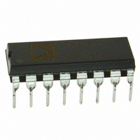
DAC8143FP Analog Devices Inc, DAC8143FP Datasheet - Page 11

DAC8143FP
Manufacturer Part Number
DAC8143FP
Description
IC DAC 12BIT DAISY-CHAIN 16-DIP
Manufacturer
Analog Devices Inc
Datasheet
1.DAC8143FSZ.pdf
(12 pages)
Specifications of DAC8143FP
Rohs Status
RoHS non-compliant
Settling Time
380ns
Number Of Bits
12
Data Interface
Serial
Number Of Converters
1
Voltage Supply Source
Single Supply
Power Dissipation (max)
500µW
Operating Temperature
-40°C ~ 85°C
Mounting Type
Through Hole
Package / Case
16-DIP (0.300", 7.62mm)
Number Of Channels
1
Resolution
12b
Interface Type
Serial (3-Wire)
Single Supply Voltage (typ)
5V
Dual Supply Voltage (typ)
Not RequiredV
Architecture
R-2R
Power Supply Requirement
Single
Output Type
Current
Integral Nonlinearity Error
±1LSB
Single Supply Voltage (min)
4.75V
Single Supply Voltage (max)
5.25V
Dual Supply Voltage (min)
Not RequiredV
Dual Supply Voltage (max)
Not RequiredV
Operating Temp Range
-40C to 85C
Operating Temperature Classification
Industrial
Mounting
Through Hole
Pin Count
16
Package Type
PDIP
Lead Free Status / Rohs Status
Not Compliant
Available stocks
Company
Part Number
Manufacturer
Quantity
Price
Part Number:
DAC8143FPZ
Manufacturer:
ADI/亚德诺
Quantity:
20 000
ANALOG/DIGITAL DIVISION
The transfer function for the DAC8143 connect in the multiply-
ing mode as shown in Figures 16 and 17 is:
where A
“OFF” bit.
The transfer function is modified when the DAC is connected in
the feedback of an operational amplifier as shown in Figure 20
and is:
The above transfer function is the division of an analog voltage
(V
bits “OFF” since division by zero is infinity. With all bits “ON”
the gain is 1 ( 1 LSB). The gain becomes 4096 with the LSB,
Bit 12, “ON”.
REV. C
Figure 19. Multiple DAC8143s with Three-Wire Interface
REF
) by a digital word. The amplifier goes to the rails with all
X
assumes a value of 1 for an “ON” bit and 0 for an
V
Figure 20. Analog/Digital Divider
IN
V
DB
WR
P
O
X
AGND
V
16
1
= –V
O
R
I
3
OUT1
2
=
FB
DAC8143
3
4
DIGITAL
INPUTS
–
+
OP-42
IN
A
2
2 12
1
1
DECODER
V
ADDRESS
SRO
2
A
V
REF
DD
1
1
A
2
ADDRESS BUS
13
DGND
6
2
2
14
15
6
A
2
–V
2
2
A
2
IN
+5V
BUFFERED DIGITAL
DATA OUT
3
3
A
2
3
3
...
SRI
SRO
SRI
SRO
SRI
SRO
SRI
SRO
...
A
2
V
12
OUT
12
STROBE
STROBE
STROBE
STROBE
DAC8143
DAC8143
DAC8143
DAC8143
LOAD
LOAD
LOAD
LOAD
A
2
12
12
–11–
APPLICATION TIPS
In most applications, linearity depends on the potential of I
I
other. In most applications, the DAC is connected to an exter-
nal op amp with its noninverting input tied to ground (see Fig-
ures 16 and 17). The amplifier selected should have a low input
bias current and low drift over temperature. The amplifier’s
input offset voltage should be nulled to less than 200 V (less
than 10% of 1 LSB).
The operational amplifier’s noninverting input should have a
minimum resistance connection to ground; the usual bias cur-
rent compensation resistor should not be used. This resistor can
cause a variable offset voltage appearing as a varying output
error. All grounded pins should tie to a single common ground
point, avoiding ground loops. The V
have a low noise level with no transients greater than +17 V.
It is recommended that the digital inputs be taken to ground or
V
mulation of static charge if the PC card is disconnected from the
system.
Peak supply current flows as the digital input pass through the
transition region (see Figure 4). The supply current decreases as
the input voltage approaches the supply rails (V
i.e., rapidly slewing logic signals that settle very near the supply
rails will minimize supply current.
INTERFACING TO THE MC6800
As shown in Figure 21, the DAC8143 may be interfaced to the
6800 by successively executing memory WRITE instruction
while manipulating the data between WRITEs, so that each
WRITE presents the next bit.
In this example, the most significant bits are found in memory
locations 0000 and 0001. The four MSBs are found in the lower
half of 0000, the eight LSBs in 0001. The data is taken from the
DB
The serial data loading is triggered by STB
a decoded memory WRITE to a memory location, R/W, and
input register to DAC register.
OUT2,
DD
2. A WRITE to another address location transfers data from
7
via a high value (1 M ) resistor; this will prevent the accu-
line.
and AGND (Pins 1, 2 and 3) being exactly equal to each
FROM SYSTEM RESET
Figure 21. DAC8143—MC6800 Interface
MC6800
*
ANALOG CIRCUITRY OMITTED FOR SIMPLICITY
R/W
DB
DB
A
A
+5V
15
2
0
0
7
16-BIT ADDRESS BUS
8-BIT DATA BUS
SRI
STB
LD
STB
STB
DD
E
E
E
1
3
2
4
1
3
2
power supply should
DAC8143*
LD
A
ADDRESS
DECODER
74LS138
0
4
2
CLR
which is asserted by
A
STB
DAC8143
2
SRO
DD
1
or DGND),
OUT1,


