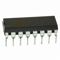
DAC8143FP Analog Devices Inc, DAC8143FP Datasheet - Page 7

DAC8143FP
Manufacturer Part Number
DAC8143FP
Description
IC DAC 12BIT DAISY-CHAIN 16-DIP
Manufacturer
Analog Devices Inc
Datasheet
1.DAC8143FSZ.pdf
(12 pages)
Specifications of DAC8143FP
Rohs Status
RoHS non-compliant
Settling Time
380ns
Number Of Bits
12
Data Interface
Serial
Number Of Converters
1
Voltage Supply Source
Single Supply
Power Dissipation (max)
500µW
Operating Temperature
-40°C ~ 85°C
Mounting Type
Through Hole
Package / Case
16-DIP (0.300", 7.62mm)
Number Of Channels
1
Resolution
12b
Interface Type
Serial (3-Wire)
Single Supply Voltage (typ)
5V
Dual Supply Voltage (typ)
Not RequiredV
Architecture
R-2R
Power Supply Requirement
Single
Output Type
Current
Integral Nonlinearity Error
±1LSB
Single Supply Voltage (min)
4.75V
Single Supply Voltage (max)
5.25V
Dual Supply Voltage (min)
Not RequiredV
Dual Supply Voltage (max)
Not RequiredV
Operating Temp Range
-40C to 85C
Operating Temperature Classification
Industrial
Mounting
Through Hole
Pin Count
16
Package Type
PDIP
Lead Free Status / Rohs Status
Not Compliant
Available stocks
Company
Part Number
Manufacturer
Quantity
Price
Part Number:
DAC8143FPZ
Manufacturer:
ADI/亚德诺
Quantity:
20 000
ESD PROTECTION
The DAC8143 digital inputs have been designed with ESD
resistance incorporated through careful layout and the inclusion
of input protection circuitry.
Figure 11 shows the input protection diodes. High voltage static
charges applied to the digital inputs are shunted to the supply
and ground rails through forward biased diodes.
These protection diodes were designed to clamp the inputs well
below dangerous levels during static discharge conditions.
EQUIVALENT CIRCUIT ANALYSIS
Figures 12 and 13 show equivalent circuits for the DAC8143’s
internal DAC with all bits LOW and HIGH, respectively. The
reference current is switched to I
and to I
source is the combination of surface and junction leakages to the
substrate. The 1/4096 current source represents the constant
1-bit current drain through the ladder’s terminating resistor.
Output capacitance is dependent upon the digital input code.
This is because the capacitance of a MOS transistor changes
with applied gate voltage. This output capacitance varies be-
tween the low and high values.
REV. C
V
V
REF
REF
I
I
REF
REF
Figure 13. Equivalent Circuit (All Inputs HIGH)
Figure 12. Equivalent Circuit (All Inputs LOW)
OUT1
R = 10k
R = 10k
DTL/TTL/CMOS
when all bits are HIGH. The I
Figure 11. Digital Input Protection
INPUTS
1/4096
1/4096
V
DD
I
I
I
I
LEAKAGE
LEAKAGE
LEAKAGE
LEAKAGE
OUT2
when all data bits are LOW,
60pF
90pF
90pF
60pF
R = 10k
R = 10k
LEAKAGE
current
R
R
I
I
I
I
OUT1
OUT2
OUT1
OUT2
FEEDBACK
FEEDBACK
–7–
DYNAMIC PERFORMANCE
ANALOG OUTPUT IMPEDANCE
The output resistance, as in the case of the output capacitance,
varies with the digital input code. This resistance, looking back
into the I
resistor alone when all digital input are LOW) and 7.5 k (the
feedback resistor in parallel with approximately 30 k of the
R-2R ladder network resistance when any single bit logic is
HIGH). Static accuracy and dynamic performance will be af-
fected by these variations.
The gain and phase stability of the output amplifier, board
layout, and power supply decoupling will all affect the dynamic
performance of the DAC8143. The use of a small compensation
capacitor may be required when high speed operational amplifi-
ers are used. It may be connected across the amplifier’s feed-
back resistor to provide the necessary phase compensation to
critically damp the output.
The considerations when using high speed amplifiers are:
1. Phase compensation (see Figures 16 and 17).
2. Power supply decoupling at the device socket and use of
OUTPUT AMPLIFIER CONSIDERATIONS
When using high speed op amps, a small feedback capacitor
(typically 5 pF–30 pF) should be used across the amplifiers to
minimize overshoot and ringing. For low speed or static
applications, ac specifications of the amplifier are not very criti-
cal. In high speed applications, slew rate, settling time, open-
loop gain and gain/phase margin specifications of the amplifier
should be selected for the desired performance. It has already
been noted that an offset can be caused by including the usual
bias current compensation resistor in the amplifier’s noninvert-
ing input terminal. This resistor should not be used. Instead, the
amplifier should have a bias current that is low over the tem-
perature range of interest.
Static accuracy is affected by the variation in the DAC’s output
resistance. This variation is best illustrated by using the circuit
of Figure 14 and the equation:
proper grounding techniques.
V
REF
OUT1
terminal, varies between 11 k (the feedback
R
2
R
Figure 14. Simplified Circuit
V
ERROR
R
2
R
= V
R
2
OS
R
1
ETC
V
R
R
OS
FB
O
DAC8143
OP-77
R
FB


