FSTUD16450MTDX Fairchild Semiconductor, FSTUD16450MTDX Datasheet
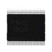
FSTUD16450MTDX

Manufacturer Part Number
FSTUD16450MTDX
Description
Manufacturer
Fairchild Semiconductor
Datasheet

Specifications of FSTUD16450MTDX

Logic Family
FST
Number Of Bits
20
Technology
CMOS
High Level Output Current
-128mA
Low Level Output Current
128mA
Propagation Delay Time
0.25ns
Package Type
TSSOP
Operating Temp Range
-40C to 85C
Operating Temperature Classification
Industrial
Operating Supply Voltage (min)
4V
Operating Supply Voltage (typ)
5V
Operating Supply Voltage (max)
5.5V
Pin Count
56
Mounting
Surface Mount
Lead Free Status / Rohs Status
Compliant
© 2001 Fairchild Semiconductor Corporation
FSTUD16450GX
(Note 1)
FSTUD16450MTD
FSTUD16450
Configurable 4-Bit to 20-Bit Bus Switch with
-2V Undershoot Protection and Selectable Level Shifting
General Description
The Fairchild Universal Bus Switch FSTUD16450 provides
4-bit, 5-bit, 8-bit, 10-bit, 16-bit, 20-bit of high-speed CMOS
TTL-compatible bus switching. The low On Resistance of
the switch allows inputs to be connected to outputs without
adding propagation delay or generating additional ground
bounce noise.
The FSTUD16450 is designed to allow “customer” configu-
ration control of the enable connections. The device is
organized as either a 4-bit, 5-bit, 10-bit or 20-bit bus switch.
8-bit and 16-bit configurations are also achievable (see
Functional Description). The device's bit configuration is
chosen through select pin logic. (see Truth Table). When
OE
HIGH, the switch is OPEN.
The A and B Ports are “undershoot hardened” with UHC®
protection to support an extended range to 2.0V below
ground. Fairchild's integrated “Undershoot
responds by preventing voltage differentials from develop-
ing and turning on the switch.
Another key device feature is the addition of a level shifting
select pin, “S
standard N-MOS switch. When S
is integrated into the circuit allowing for level shifting
between 5V inputs and 3.3V outputs.
Ordering Code:
Devices also available in Tape and Reel. Specify by appending the suffix letter “X” to the ordering code.
Note 1: BGA package available in Tape and Reel only.
UHC® is a registered trademark of Fairchild Semiconductor Corporation.
Circuit” (UHC) senses undershoot at the I/Os, and
Order Number
x
is LOW, Port A
2
”. When S
x
Package Number
is connected to Port B
(Preliminary)
2
BGA54A
MTD56
is LOW, the device behaves as a
2
is HIGH, a diode to V
54-Ball Fine-Pitch Ball Grid Array (FBGA), JEDEC MO-205, 5.5mm Wide
[Tape and Reel]
56-Lead Thin Shrink Small Outline Package (TSSOP), JEDEC MO-153, 6.1mm Wide
x
. When OE
DS500391
Hardened
x
CC
is
Features
Applications Note
Select pins S
user configurable control pins. The AC performance of
these pins has not been characterized or tested. Switching
of these select pins during system operation may tempo-
rarily disrupt output logic states and/or enable pin controls.
Undershoot hardened to 2V (A and B Ports)
Voltage level shifting
4 switch connection between two ports
Minimal propagation delay through the switch
Low l
Zero bounce in flow-through mode
Control inputs compatible with TTL level
See Applications Note AN-5008 for details
Also packaged in plastic Fine-Pitch Ball Grid Array
(FBGA) (Preliminary)
CC
Package Description
0
, S
1
, S
2
are intended to be used as static
January 2001
Revised October 2006
www.fairchildsemi.com

Related parts for FSTUD16450MTDX

FSTUD16450MTDX Summary of contents

Page 1

... Thin Shrink Small Outline Package (TSSOP), JEDEC MO-153, 6.1mm Wide Devices also available in Tape and Reel. Specify by appending the suffix letter “X” to the ordering code. Note 1: BGA package available in Tape and Reel only. UHC® registered trademark of Fairchild Semiconductor Corporation. © 2001 Fairchild Semiconductor Corporation Features ...

Page 2

Connection Diagrams Pin Assignment for TSSOP Pin Assignment for FBGA (Top Thru View) www.fairchildsemi.com Pin Descriptions Pin Name Description Bus Switch Enables 1 2 1A, 2A Bus A 1B, 2B Bus Bit Configuration ...

Page 3

Logic Diagrams 20-Bit Configuration (Configuration 1) 5-Bit Configuration (Configuration 3) 10-Bit Configuration (Configuration 2) 4-Bit Configuration (Configuration 4) 3 www.fairchildsemi.com ...

Page 4

Functional Description The device can also be configured and 16-bit device by grounding the unused pins in Configurations 2 and 1 respectively. The 8-bit configuration may also be achieved by tying two of the 4-bit enables from ...

Page 5

Truth Tables (Continued Configuration Inputs ...

Page 6

Absolute Maximum Ratings Supply Voltage ( Switch Voltage (V ) (Note Input Control Pin Voltage (V ) (Note Input Diode Current ( Output (I ) ...

Page 7

AC Electrical Characteristics Symbol Parameter Propagation Delay Bus-to-Bus PHL PLH (Note Output Enable Time PZH PZL Output Disable Time PHZ PLZ Output ...

Page 8

Undershoot Characteristic Symbol Parameter V Output Voltage During Undershoot OUTU Note 11: This test is intended to characterize the device’s protective capabilities by maintaining output signal integrity during an input transient voltage undershoot event. Device Test Conditions Parameter Value V ...

Page 9

FIGURE 4. 9 www.fairchildsemi.com ...

Page 10

Physical Dimensions inches (millimeters) unless otherwise noted 54-Ball Fine-Pitch Ball Grid Array (FBGA), JEDEC MO-205, 5.5mm Wide www.fairchildsemi.com Package Number BGA54A Preliminary 10 ...

Page 11

Physical Dimensions inches (millimeters) unless otherwise noted (Continued) 56-Lead Thin Shrink Small Outline Package (TSSOP), JEDEC MO-153, 6.1mm Wide Technology Description The Fairchild Switch family derives from and embodies Fairchild’s proven switch technology used for several years in its 74LVX3L384 ...

Related keywords