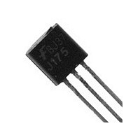
J175NL Fairchild Semiconductor, J175NL Datasheet - Page 10

J175NL
Manufacturer Part Number
J175NL
Description
Manufacturer
Fairchild Semiconductor
Datasheet
1.J175NL.pdf
(12 pages)
Specifications of J175NL
Channel Type
P
Configuration
Single
Gate-source Voltage (max)
30V
Drain-gate Voltage (max)
-30V
Operating Temperature (min)
-55C
Operating Temperature (max)
150C
Operating Temperature Classification
Military
Mounting
Through Hole
Pin Count
3
Package Type
TO-92
Lead Free Status / Rohs Status
Compliant
SOT-23 Tape and Reel Data, continued
SOT-23 Reel Configuration: Figure 4.0
Notes: A0, B0, and K0 dimensions are determined with respect to the EIA/Jedec RS-481
SOT-23 Embossed Carrier Tape
Configuration: Figure 3.0
Tape Size
8mm
8mm
B0
Pkg type
SOT-23
(8mm)
Dim A
max
rotational and lateral movement requirements (see sketches A, B, and C).
K0
7" Dia
13" Dia
T
Tc
Option
Wc
3.15
+/-0.10
Reel
A0
20 deg maximum component rotation
13" Diameter Option
2.77
+/-0.10
7.00
177.8
13.00
330
Dim A
B0
Sketch A (Side or Front Sectional View)
Component Rotation
8.0
+/-0.3
0.059
1.5
0.059
1.5
Dim B
W
1.55
+/-0.05
512 +0.020/-0.008
13 +0.5/-0.2
512 +0.020/-0.008
13 +0.5/-0.2
P0
D0
Dimensions are in inches and millimeters
Dim C
P1
1.125
+/-0.125
User Direction of Feed
D1
See detail AA
Dimensions are in millimeter
W2 max Measured at Hub
P2
1.75
+/-0.10
E1
Dim N
0.795
20.2
0.795
20.2
Dim D
W1 Measured at Hub
B0
A0
Sketch B (Top View)
Component Rotation
6.25
min
D0
E2
2.165
55
4.00
100
Dim N
A0
W3
3.50
+/-0.05
20 deg maximum
D1
F
0.331 +0.059/-0.000
8.4 +1.5/0
0.331 +0.059/-0.000
8.4 +1.5/0
Dim A
Typical
component
cavity
center line
Typical
component
center line
Dim D
Max
min
4.0
+/-0.1
Dim W1
P1
4.0
+/-0.1
7" Diameter Option
P0
DETAIL AA
Dim W2
0.567
14.4
0.567
14.4
1.30
+/-0.10
K0
Sketch C (Top View)
Component lateral movement
0.5mm
maximum
F
E1
E2
0.228
+/-0.013
0.311 – 0.429
7.9 – 10.9
0.311 – 0.429
7.9 – 10.9
Dim W3 (LSL-USL)
W
T
B Min
September 1999, Rev. C
Dim C
See detail AA
0.5mm
maximum
5.2
+/-0.3
Wc
0.06
+/-0.02
Tc


