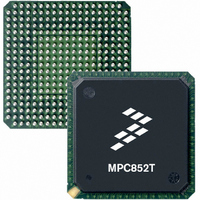
MPC852TCVR100A Freescale Semiconductor, MPC852TCVR100A Datasheet - Page 57

MPC852TCVR100A
Manufacturer Part Number
MPC852TCVR100A
Description
IC MPU POWERQUICC 100MHZ 256PBGA
Manufacturer
Freescale Semiconductor
Datasheet
1.MPC852TVR50A.pdf
(80 pages)
Specifications of MPC852TCVR100A
Processor Type
MPC8xx PowerQUICC 32-Bit
Speed
100MHz
Voltage
1.8V
Mounting Type
Surface Mount
Package / Case
256-PBGA
Processor Series
MPC8xx
Core
MPC8xx
Data Bus Width
32 bit
Development Tools By Supplier
MPC852TADS-KIT
Maximum Clock Frequency
100 MHz
Operating Supply Voltage
0 V to 3.3 V
Maximum Operating Temperature
+ 105 C
Mounting Style
SMD/SMT
Data Ram Size
8 KB
Minimum Operating Temperature
- 40 C
Program Memory Size
4 KB
Program Memory Type
EPROM/Flash
Lead Free Status / RoHS Status
Lead free / RoHS Compliant
Features
-
Lead Free Status / Rohs Status
Details
Available stocks
Company
Part Number
Manufacturer
Quantity
Price
Company:
Part Number:
MPC852TCVR100A
Manufacturer:
FREESCAL
Quantity:
300
Company:
Part Number:
MPC852TCVR100A
Manufacturer:
Freescale Semiconductor
Quantity:
10 000
15 FEC Electrical Characteristics
This section provides the AC electrical specifications for the fast Ethernet controller (FEC). Note that the
timing specifications for the MII signals are independent of system clock frequency (part speed
designation). Also, MII signals use TTL signal levels compatible with devices operating at either 5.0 V or
3.3 V.
15.1
The receiver functions correctly up to a MII_RX_CLK maximum frequency of 25MHz +1%. There is no
minimum frequency requirement. In addition, the processor clock frequency must exceed the
MII_RX_CLK frequency –1%.
Table 25
Figure 59
15.2
The transmitter functions correctly up to a MII_TX_CLK maximum frequency of 25 MHz + 1%. There is
no minimum frequency requirement. In addition, the processor clock frequency must exceed the
MII_TX_CLK frequency – 1%.
Freescale Semiconductor
Num
M1
M2
M3
M4
provides information on the MII receive signal timing.
MII_RXD[3:0] (Inputs)
MII_RXD[3:0], MII_RX_DV, MII_RX_ER to MII_RX_CLK setup
MII_RX_CLK to MII_RXD[3:0], MII_RX_DV, MII_RX_ER hold
MII_RX_CLK pulse width high
MII_RX_CLK pulse width low
MII Receive Signal Timing (MII_RXD[3:0], MII_RX_DV, MII_RX_ER,
MII_RX_CLK)
MII Transmit Signal Timing (MII_TXD[3:0], MII_TX_EN,
MII_TX_ER, MII_TX_CLK)
shows MII receive signal timing.
MII_RX_CLK (Input)
MII_RX_ER
MII_RX_DV
MPC852T PowerQUICC™ Hardware Specifications, Rev. 4
Figure 59. MII Receive Signal Timing Diagram
Characteristic
Table 25. MII Receive Signal Timing
M1
M2
M3
35%
35%
M4
Min
5
5
Max
65%
65%
—
—
FEC Electrical Characteristics
MII_RX_CLK period
MII_RX_CLK period
Unit
ns
ns
57


