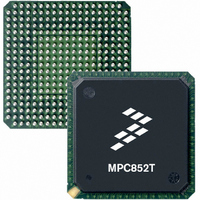
MPC852TCVR100A Freescale Semiconductor, MPC852TCVR100A Datasheet - Page 76

MPC852TCVR100A
Manufacturer Part Number
MPC852TCVR100A
Description
IC MPU POWERQUICC 100MHZ 256PBGA
Manufacturer
Freescale Semiconductor
Datasheet
1.MPC852TVR50A.pdf
(80 pages)
Specifications of MPC852TCVR100A
Processor Type
MPC8xx PowerQUICC 32-Bit
Speed
100MHz
Voltage
1.8V
Mounting Type
Surface Mount
Package / Case
256-PBGA
Processor Series
MPC8xx
Core
MPC8xx
Data Bus Width
32 bit
Development Tools By Supplier
MPC852TADS-KIT
Maximum Clock Frequency
100 MHz
Operating Supply Voltage
0 V to 3.3 V
Maximum Operating Temperature
+ 105 C
Mounting Style
SMD/SMT
Data Ram Size
8 KB
Minimum Operating Temperature
- 40 C
Program Memory Size
4 KB
Program Memory Type
EPROM/Flash
Lead Free Status / RoHS Status
Lead free / RoHS Compliant
Features
-
Lead Free Status / Rohs Status
Details
Available stocks
Company
Part Number
Manufacturer
Quantity
Price
Company:
Part Number:
MPC852TCVR100A
Manufacturer:
FREESCAL
Quantity:
300
Company:
Part Number:
MPC852TCVR100A
Manufacturer:
Freescale Semiconductor
Quantity:
10 000
Document Revision History
17 Document Revision History
Table 32
76
Revision
3.1
3.0
2.0
1.8
1.7
1.6
1.5
1.4
1.3
1.2
1.1
4
1
0
lists significant changes between revisions of this document.
1/18/2005 Document template update.
11/2004
12/2003
12/2002
11/2002
10/2002
7/2003
5/2003
4/2003
4/2003
2/2003
1/2003
1/2003
Date
Put 852T on the 1st page in place of 8245.
Figure 62 on page 59 had overbars added on signals CR (pin G2) and WAIT_A (pin P4).
Changed the pinout to be JEDEC Compliant, changed timing parameters B28a through B28d, and
B29d to show that TRLX can be 0 or 1.
Changed the SPI Master Timing Specs. 162 and 164
Changed the package drawing in Figure 15-63
Changed 5 Port C pins with interrupt capability to 7 Port C pins. Added the Note: solder sphere
composition for MPC852TVR and MPC852TCVR devices is 95.5%Sn 45%Ag 0.5%Cu to Figure
15-63
Changed Table 15-30 Pin Assignments for the PLL Pins V
Added subscripts to timing diagrams for B1-B35, to specify memory controller settings for the specific
edges.
In Table 15-30, specified EXTCLK as 3.3 V.
Added fast Ethernet controller to the features
Added values for 80 and 100 MHz
Initial release
• Updated template.
• On page 1, updated first paragraph and added a second paragraph.
• After Table 2, inserted a new figure showing the undershoot/overshoot voltage
• In
• In
• In
• In
• Added sentence to Spec B1A about EXTCLK and CLKOUT being in Alignment for Integer Values
• Added a footnote to Spec 41 specifying that EDM = 1
• Broke the
renumbered the rest of the figures.
to bus operation up to 50 MHz.
pinouts.
Table
Figure
Table
Figure
MPC852T PowerQUICC™ Hardware Specifications, Rev. 4
9, for reset timings B29f and B29g added footnote indicating that the formula only applies
17, changed num 46 description to read, “TA assertion to rising edge ...”
4, changed all reference voltage measurement points from 0.2 and 0.8 V to 50% level.
42, changed TA to reflect the rising edge of the clock.
Section 16.1, “Pin
Table 32. Document Revision History
Assignments,” into 2 smaller sections for the JEDEC and non-JEDEC
Changes
SSSYN1
, V
SSSYN
, V
Freescale Semiconductor
DDSYN
(Figure
2) and


