MPC8321CVRADDC Freescale Semiconductor, MPC8321CVRADDC Datasheet - Page 7
MPC8321CVRADDC
Manufacturer Part Number
MPC8321CVRADDC
Description
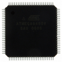
IC MPU PWRQUICC II 516-PBGA
Manufacturer
Freescale Semiconductor
Series
PowerQUICC II PROr
Datasheet
1.MPC8321VRADDC.pdf
(82 pages)
Specifications of MPC8321CVRADDC
Processor Type
MPC83xx PowerQUICC II Pro 32-Bit
Speed
266MHz
Voltage
1V
Mounting Type
Surface Mount
Package / Case
516-PBGA
Processor Series
MPC8xxx
Core
e300
Data Bus Width
32 bit
Development Tools By Supplier
MPC8323E-MDS-PB
Maximum Clock Frequency
266 MHz
Maximum Operating Temperature
+ 105 C
Mounting Style
SMD/SMT
Data Ram Size
16 KB
I/o Voltage
1.8 V, 3.3 V
Interface Type
I2C, SPI, UART
Minimum Operating Temperature
- 40 C
Core Size
32 Bit
Program Memory Size
32KB
Cpu Speed
266MHz
Embedded Interface Type
I2C, SPI, USB, UART
Digital Ic Case Style
BGA
No. Of Pins
516
Rohs Compliant
Yes
Lead Free Status / RoHS Status
Lead free / RoHS Compliant
Features
-
Lead Free Status / Rohs Status
Lead free / RoHS Compliant
Available stocks
Company
Part Number
Manufacturer
Quantity
Price
Company:

Part Number:
MPC8321CVRADDC
Manufacturer:
Freescale Semiconductor
Quantity:
135
Company:
Part Number:
MPC8321CVRADDC
Manufacturer:
Freescale Semiconductor
Quantity:
10 000
Company:
Part Number:
MPC8321CVRADDCA
Manufacturer:
FREESCA
Quantity:
6


2.1.2
Table 2
recommended and tested operating conditions. Proper device operation outside of these conditions is not
guaranteed.
Figure 2
Freescale Semiconductor
Core supply voltage
PLL supply voltage
DDR1 and DDR2 DRAM I/O voltage
PCI, local bus, DUART, system control and power management,
I
Junction temperature
Note:
1. GV
2. Minimum temperature is specified with T
3. All IO pins should be interfaced with peripherals operating at same voltage level.
4. This voltage is the input to the filter discussed in
2
C, SPI, and JTAG I/O voltage
direction.
at the AVDD pin, which may be reduced due to voltage drop across the filter.
MPC8323E PowerQUICC II Pro Integrated Communications Processor Family Hardware Specifications, Rev. 4
DD
, OV
provides the recommended operating conditions for the MPC8323E. Note that these values are the
shows the undershoot and overshoot voltages at the interfaces of the MPC8323E
DD
Power Supply Voltage Specification
, AV
DD
V
V
Note:
, and V
1. t
IH
IL
Characteristic
interface
DD
G/OV
Figure 2. Overshoot/Undershoot Voltage for GV
G/OV
GND – 0.3 V
GND – 0.7 V
must track each other and must vary in the same direction—either in the positive or negative
refers to the clock period associated with the bus clock interface.
DD
Table 2. Recommended Operating Conditions
DD
G/OV
+ 20%
+ 5%
GND
DD
A
; maximum temperature is specified with T
Section 24.2, “PLL Power Supply
Not to Exceed 10%
of t
Symbol
GV
OV
AV
interface
T
V
A
DD
/T
DD
DD
DD
J
1
Filtering” and not necessarily the voltage
Recommended
2.5 V ± 125 mV
3.3 V ± 300 mV
1.0 V ± 50 mV
1.0 V ± 50 mV
1.8 V ± 90 mV
DD
J
.
0 to 105
/OV
3
Value
DD
Electrical Characteristics
Unit
°C
V
V
V
V
Notes
1
1
1
1
2
7
Related parts for MPC8321CVRADDC
Image
Part Number
Description
Manufacturer
Datasheet
Request
R

Part Number:
Description:
Manufacturer:
Freescale Semiconductor, Inc
Datasheet:
Part Number:
Description:
Manufacturer:
Freescale Semiconductor, Inc
Datasheet:
Part Number:
Description:
Manufacturer:
Freescale Semiconductor, Inc
Datasheet:
Part Number:
Description:
Manufacturer:
Freescale Semiconductor, Inc
Datasheet:
Part Number:
Description:
Manufacturer:
Freescale Semiconductor, Inc
Datasheet:
Part Number:
Description:
Manufacturer:
Freescale Semiconductor, Inc
Datasheet:
Part Number:
Description:
Manufacturer:
Freescale Semiconductor, Inc
Datasheet:
Part Number:
Description:
Manufacturer:
Freescale Semiconductor, Inc
Datasheet:
Part Number:
Description:
Manufacturer:
Freescale Semiconductor, Inc
Datasheet:
Part Number:
Description:
Manufacturer:
Freescale Semiconductor, Inc
Datasheet:
Part Number:
Description:
Manufacturer:
Freescale Semiconductor, Inc
Datasheet:
Part Number:
Description:
Manufacturer:
Freescale Semiconductor, Inc
Datasheet:
Part Number:
Description:
Manufacturer:
Freescale Semiconductor, Inc
Datasheet:
Part Number:
Description:
Manufacturer:
Freescale Semiconductor, Inc
Datasheet:
Part Number:
Description:
Manufacturer:
Freescale Semiconductor, Inc
Datasheet: