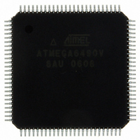
MPC8321CVRADDC Freescale Semiconductor, MPC8321CVRADDC Datasheet - Page 9

MPC8321CVRADDC
Manufacturer Part Number
MPC8321CVRADDC
Description
IC MPU PWRQUICC II 516-PBGA
Manufacturer
Freescale Semiconductor
Series
PowerQUICC II PROr
Datasheet
1.MPC8321VRADDC.pdf
(82 pages)
Specifications of MPC8321CVRADDC
Processor Type
MPC83xx PowerQUICC II Pro 32-Bit
Speed
266MHz
Voltage
1V
Mounting Type
Surface Mount
Package / Case
516-PBGA
Processor Series
MPC8xxx
Core
e300
Data Bus Width
32 bit
Development Tools By Supplier
MPC8323E-MDS-PB
Maximum Clock Frequency
266 MHz
Maximum Operating Temperature
+ 105 C
Mounting Style
SMD/SMT
Data Ram Size
16 KB
I/o Voltage
1.8 V, 3.3 V
Interface Type
I2C, SPI, UART
Minimum Operating Temperature
- 40 C
Core Size
32 Bit
Program Memory Size
32KB
Cpu Speed
266MHz
Embedded Interface Type
I2C, SPI, USB, UART
Digital Ic Case Style
BGA
No. Of Pins
516
Rohs Compliant
Yes
Lead Free Status / RoHS Status
Lead free / RoHS Compliant
Features
-
Lead Free Status / Rohs Status
Lead free / RoHS Compliant
Available stocks
Company
Part Number
Manufacturer
Quantity
Price
Company:
Part Number:
MPC8321CVRADDC
Manufacturer:
Freescale Semiconductor
Quantity:
135
Company:
Part Number:
MPC8321CVRADDC
Manufacturer:
Freescale Semiconductor
Quantity:
10 000
Company:
Part Number:
MPC8321CVRADDCA
Manufacturer:
FREESCA
Quantity:
6
DDR I/O
65% utilization
2.5 V
R
R
1 pair of clocks
3
The estimated typical power dissipation for this family of MPC8323E devices is shown in
Table 6
Freescale Semiconductor
Notes:
1. The values do not include I/O supply power (OV
2. Typical power is based on a nominal voltage of V
3. Maximum power is based on a voltage of V
s
t
= 50 Ω
Frequency (MHz)
= 20 Ω
benchmark application. The measurements were taken on the MPC8323MDS evaluation board using WC process silicon.
MPC8323E PowerQUICC II Pro Integrated Communications Processor Family Hardware Specifications, Rev. 4
Interface
Power Characteristics
CSB
shows the estimated typical I/O power dissipation for the device.
133
133
90%
V
Frequency (MHz)
0
QUICC Engine
266 MHz, 1 × 32 bits
PORESET
Figure 3. MPC8323E Power-Up Sequencing Example
200
200
Table 6. Estimated Typical I/O Power Dissipation
Parameter
Table 5. MPC8323E Power Dissipation
DD
= 1.07 V, WC process, a junction T
Frequency (MHz)
DD
DD
and GV
= 1.0 V, ambient temperature, and the core running a Dhrystone
Core
GV
266
333
DD
0.212
DD
(1.8 V)
) or AV
I/O Voltage (GV
>= 32 clocks x t
DD
GV
. For I/O power values, see
Typical
Core Voltage (V
DD
0.74
0.78
0.367
(2.5 V) OV
DD
SYS_CLK_IN
J
and OV
= 110°C, and an artificial smoke test.
Maximum
DD
DD
1.48
1.62
DD
—
)
0.7 V
/t
(3.3 V) Unit
PCI_SYNC_IN
)
Table
t
W
Power Characteristics
Unit
W
W
6.
Table
Comments
—
5.
Notes
1, 2, 3
1, 2, 3
9


