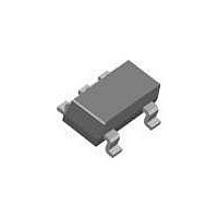
ILC7080AIM550X Fairchild Semiconductor, ILC7080AIM550X Datasheet - Page 5

ILC7080AIM550X
Manufacturer Part Number
ILC7080AIM550X
Description
Low Dropout (LDO) Regulators 0.08A LDO
Manufacturer
Fairchild Semiconductor
Datasheet
1.ILC7080AIM526X.pdf
(16 pages)
Specifications of ILC7080AIM550X
Number Of Outputs
1
Polarity
Positive
Input Voltage Max
13 V
Output Voltage
5 V
Output Type
Fixed
Dropout Voltage (max)
150 mV
Output Current
500 mA
Line Regulation
0.032 % / V
Load Regulation
50 mV
Voltage Regulation Accuracy
1 %
Maximum Power Dissipation
0.25 W
Maximum Operating Temperature
+ 85 C
Mounting Style
SMD/SMT
Package / Case
SOT-23-5
Minimum Operating Temperature
- 40 C
Lead Free Status / Rohs Status
Lead free / RoHS Compliant
Shutdown (ON/OFF) Operation
The ILC7080/81 output can be turned off by applying 0.4V
or less to the device’s ON/OFF pin (pin 3). In shutdown
mode, the ILC7080/81 draws less than 1µA quiescent cur-
rent. The output of the ILC7081 is enabled by applying 2V to
13V at the ON/OFF pin. In applications where the ILC7080/
81 output will always remain enabled, the ON/OFF pin may
be connected to V
circuitry includes hysteresis, as such the device will operate
properly even if a slow moving signal is applied to the ON/
OFF pin.
Short Circuit Protection
The ILC7080/81 output can withstand momentary short
circuit to ground. Moreover, the regulator can deliver very
high output peak current due to its 1A instantaneous short
circuit current capability.
Thermal Protection
The ILC7080/81 also includes a thermal protection circuit
which shuts down the regulator when die temperature
exceeds 150˚C due to overheating. In thermal shutdown,
once the die temperature cools to below 140˚C, the regulator
is enabled. If the die temperature is excessive due to high
package power dissipation, the regulator’s thermal circuit
will continue to pulse the regulator on and off. This is called
thermal cycling.
Excessively high die temperature may occur due to high
differential voltage across the regulator or high load current
or high ambient temperature or a combination of all three.
Thermal protection protects the regulator from such fault
conditions and is a necessary requirement in today’s designs.
In normal operation, the die temperature should be limited to
under 150˚C.
REV. 1.0.7 4/3/03
IN
(pin 1). The ILC7080/81’s shutdown
Figure 2. ILC7080/81 RF LDO regulator block diagram
V
C
GND
ON/OFF
IN
NOISE
REFERENCE
BANDGAP
V
REF
AMPLIFIER
ERROR
INTERNAL V
FEEDBACK
Adjustable Output Voltage
Figure 3 shows how an adjustable output voltage can be
easily achieved using ILC7081-ADJ. The output voltage,
V
V
Figure 3. Application circuit for adjustable output voltage
For best results, a resistor value of 470kΩ or less may be
used for R2. The output voltage can be programmed from
2.5V to 12V.
Note: An external capacitor should not be connected to the
adjustable feedback pin (pin 4). Connecting an external
capacitor to pin 4 may cause regulator instability and lead to
oscillations.
OUT
OUT
DD
CONDUCTANCE
is given by the following equation:
= 1.24V x (R1/R2 + 1)
AMPLIFIER
TRANS-
V
V
C
OUT
IN
OUT
C
IN
V
OUT
5
1
ILC7081-ADJ
SOT23-5
R
1
2
4
3
ON
V
R
ADJ
2
OFF
ILC7080/81
5


