DP83849CVS/NOPB National Semiconductor, DP83849CVS/NOPB Datasheet - Page 63
DP83849CVS/NOPB
Manufacturer Part Number
DP83849CVS/NOPB
Description
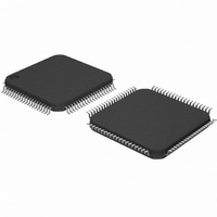
IC TXRX ETHERNET PHY DUAL 80TQFP
Manufacturer
National Semiconductor
Type
Transceiverr
Specifications of DP83849CVS/NOPB
Number Of Drivers/receivers
2/2
Protocol
Ethernet
Voltage - Supply
3 V ~ 3.6 V
Mounting Type
Surface Mount
Package / Case
80-TQFP, 80-VQFP
Data Rate
100Mbps
Supply Voltage Range
3V To 3.6V
Logic Case Style
TQFP
No. Of Pins
80
Operating Temperature Range
0°C To +70°C
Msl
MSL 3 - 168 Hours
Filter Terminals
SMD
Rohs Compliant
Yes
Data Rate Max
10Mbps
For Use With
DP83849CVS-EVK - BOARD EVALUATION DP83849CVS
Lead Free Status / RoHS Status
Lead free / RoHS Compliant
Other names
*DP83849CVS
*DP83849CVS/NOPB
DP83849CVS
*DP83849CVS/NOPB
DP83849CVS
Available stocks
Company
Part Number
Manufacturer
Quantity
Price
Company:

Part Number:
DP83849CVS/NOPB
Manufacturer:
NS
Quantity:
618
Company:
Part Number:
DP83849CVS/NOPB
Manufacturer:
Texas Instruments
Quantity:
10 000


7.2.4 RMII and Bypass Register (RBR)
This register configures the RMII/MII Interface Mode of operation. This register controls selecting MII or RMII mode for
Receive or Transmit. In addition, several additional bits are included to allow datapath selection for Transmit and Receive
in multiport applications.
12:9
Bit
7:6
1:0
15
14
13
8
5
4
3
2
ELAST_BUF[1:0]
RX_OVF_STS
RX_UNF_STS
RMII_REV1_0
DIS_TX_OPT
SIM_WRITE
PMD_LOOP
RMII_MODE
RESERVED
RESERVED
RESERVED
Bit Name
Table 36. RMII and Bypass Register (RBR), addresses 17h
0, RO/COR
0, RO/COR
Strap, RW
Default
01, RW
0, RW
0, RW
0, RW
0, RW
0, RO
0
0
Simultaneous Write:
Setting this bit in port A register space enables simultaneous write
to Phy registers in both ports. Subsequent writes to port A registers
will write to registers in both ports A and B.
1 = Simultaneous writes to both ports
0 = Per-port write
RESERVED: Writes ignored, Read as 0
Disable RMII TX Latency Optimization:
Normally the RMII Transmitter will minimize the transmit latency by
realigning the transmit clock with the Reference clock phase at the
start of a packet transmission. Setting this bit will disable Phase re-
alignment and ensure that IDLE bits will always be sent in multiples
of the symbol size. This will result in a larger uncertainty in RMII
transmit latency.
RESERVED:
Must be zero
PMD Loopback:
0= Normal Operation
1= Remote (PMD) Loopback
Setting this bit will cause the device to Loopback data received
from the Physical Layer. The loopback is done prior to the MII or
RMII interface. Data received at the internal MII or RMII interface
will be applied to the transmitter. This mode should only be used if
RMII mode is enabled.
RESERVED:
Must be zero
Reduced MII Mode:
0 = Standard MII Mode
1 = Reduced MII Mode
Reduced MII Revision 1.0:
0 = (RMII revision 1.2) CRS_DV will toggle at the end of a packet
to indicate deassertion of CRS.
1 = (RMII revision 1.0) CRS_DV will remain asserted until final data
is transferred. CRS_DV will not toggle at the end of a packet.
RX FIFO Over Flow Status:
0 = Normal
1 = Overflow detected
RX FIFO Under Flow Status:
0 = Normal
1 = Underflow detected
Receive Elasticity Buffer:
This field controls the Receive Elasticity Buffer which allows for fre-
quency variation tolerance between the 50MHz RMII clock and the
recovered data. See Section 3.2 for more information on Elasticity
Buffer settings in RMII mode.
63
Description
www.national.com
Related parts for DP83849CVS/NOPB
Image
Part Number
Description
Manufacturer
Datasheet
Request
R

Part Number:
Description:
National Semiconductor [8-Bit D/A Converter]
Manufacturer:
National Semiconductor
Datasheet:
Part Number:
Description:
National Semiconductor [Media Coprocessor]
Manufacturer:
National Semiconductor
Datasheet:
Part Number:
Description:
Digitally Controlled Tone and Volume Circuit with Stereo Audio Power Amplifier, Microphone Preamp Stage and National 3D Sound
Manufacturer:
National Semiconductor
Datasheet:
Part Number:
Description:
Digitally Controlled Tone and Volume Circuit with Stereo Audio Power Amplifier, Microphone Preamp Stage and National 3D Sound
Manufacturer:
National Semiconductor
Datasheet:
Part Number:
Description:
AC97 Rev 2 Codec with Sample Rate Conversion and National 3D Sound
Manufacturer:
National Semiconductor
Part Number:
Description:
Manufacturer:
National Semiconductor
Datasheet:
Part Number:
Description:
Manufacturer:
National Semiconductor
Datasheet:
Part Number:
Description:
General Purpose, Low Voltage, Low Power, Rail-to-Rail Output Operational Amplifiers
Manufacturer:
National Semiconductor
Datasheet:
Part Number:
Description:
8-bit 20 MSPS flash A/D converter.
Manufacturer:
National Semiconductor
Datasheet:
Part Number:
Description:
Low Noise Quad Operational Amplifier
Manufacturer:
National Semiconductor
Datasheet:
Part Number:
Description:
Quad Differential Line Receivers
Manufacturer:
National Semiconductor
Datasheet:
Part Number:
Description:
Quad High Speed Trapezoidal? Bus Transceiver
Manufacturer:
National Semiconductor
Datasheet:
Part Number:
Description:
Dual Line Receiver
Manufacturer:
National Semiconductor
Datasheet:
Part Number:
Description:
TTL to 10k ECL Level Translator with Latch
Manufacturer:
National Semiconductor
Datasheet: