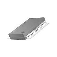
KA2822D Fairchild Semiconductor, KA2822D Datasheet

KA2822D
Specifications of KA2822D
Available stocks
Related parts for KA2822D
KA2822D Summary of contents
Page 1
... Typical Application • 3.5-inch floppy disk drive (FDD) spildle motor • Other 3-phase BLDC motor ©2000 Fairchild Semiconductor International Description The KA2822D is a monolithic integrated circuit, and suit- able for the three-phase spindle motor driver of FDD system. 28-SSOPH-375 : 1A) PEAK Ordering Information ...
Page 2
... FG INPUT( ) AGC INDEX PULSE WIDTH VOLTAGE REG INDEX BURST INDEX OUTPUT CE SIGNAL GROUND FG ZERO CROSS FG OUTPUT RPM SELECT CHARGE PUMP OUTPUT OSC INPUT KA2822D FIN INPUT(+) HALL BIAS CURRENT DETECTION1 V INPUT INPUT(+) U PHASE OUTPUT V PHASE OUTPUT FIN W PHASE OUTPUT NC U INPUT(+) ...
Page 3
... W phase output pin O V phase output pin O U phase output pin I Positive input pin of V phase amp I Negative input pin of V phase amp I Over current detection pin I Hall sensor bias input pin I Positive input pin of FG signal amp - Power ground 3 KA2822D ...
Page 4
... KA2822D Internal Block Diagram U INPUT (+) 19 + U_AMP U INPUT INPUT (+) 24 + V_AMP V INPUT AGC AGC 2 HALL BIAS Start- 1.3V FG_AMP FG INPUT(+) INPUT OUTPUT 9 FG ZERO CROSS Timing Detectpr VOLTAGE REG. 4 2.2V 5 INDEX BURST 13 OSC INPUT OSC 14 NC CURRENT V DETECTION2 Output Control Hall Zero-cross CON_AMP ...
Page 5
... drive output and current detection 1, 2 vcc 5k 2.5k (18Pin, 24Pin) 40k vcc (28Pin) (13Pin) vcc vcc (10Pin) Hall bias input and voltage regulator output vcc (27Pin) 5 KA2822D (17Pin, 26Pin (16Pin (23Pin) (22Pin) W (21Pin) 40k 40k OSC input vcc 0.1k 1k 50pF 5k ...
Page 6
... KA2822D Equivalent Circuits (Continued) Index pulse width detection output vcc vcc 2k 2k RPM select input vcc 6k (11Pin) Index output vcc (6Pin) Phase compensation and current detection 1, 2 vcc (15Pin) (3Pin) vcc AGC (2Pin) vcc 1.4V 6 vcc vcc vcc vcc vcc (17Pin, ...
Page 7
... Equivalent Circuits (Continued) (9Pin) vcc to IIL Circuit Charge pump FG zero cross output vcc vcc vcc Charge pump output vcc (12Pin) vcc 7 KA2822D vcc Buffer amp ...
Page 8
... KA2822D Absolute Maximum Rating (Ta=25 C) Parameter Maximum power supply voltage Maximum input voltage Maximum output current Normal output current Power dissipation Operating temperature Junction temperture Storage temperature Power Dissipation Curve Power Dissipation : PD[W] Power dissipation decreases in the rate of 13.5mV / C when mounted on 50mm rial) and used above Ta=25 C ...
Page 9
... N note V - COM V - DIF V I =4mA, CE=L HB1 =10mA, CE=L HB2 H Vref I =1mA, CE =7V, CE=H HOFF CER Vsat1 I =0.35A O Vsat2 I =0. CT1 Vref1 Current limiter voltage Vref2 Control begin voltage 9 KA2822D Min. Typ. Max. Units - 1.0 2 1 1 100 ...
Page 10
... KA2822D Electrical Characteristics (Continued) (Ta= =5V) CC Parameter CHARGE PUMP Charge current Discharge current note Current ratio Off current note Clamp voltage FG AMP note Output DC voltage Voltage gain 2 note Input voltage range note Noise margin 1 note Noise margin 2 SPEED CONTROL note Count range 1 ...
Page 11
... This function compares the real motor rotation frequency with the 300 or 360Hz pulse divided from 1MHz clock pulse for removing speed error when motor is on and speed error is detected by PLL. The speed error sent to charge pump part which repeats charge and discharge controls the output current of the output amp to keep a stable rotation. 11 KA2822D ...
Page 12
... KA2822D Typical Performance Characteristics I CC 15.0 [mA] 1.5 /div Vref 3.0 [V] 0.3 /div. 0 0.8/div vs. Vref (Pin4) CC 0.8/div vs Index pulse width 8.0 [ms] 1.0 /div. 0 4.2 4.5 5.0 5.5 8.0[V] V vs. Index pulse width CC 12 8.0[V] 8.0[V] 6.0 6.5 7.0 7 ...
Page 13
... HALL BIAS 27 AGC 2 CE KA2822D 7 FG_INPUT(+) 28 FG_INPUT(-) 1 FG ZERO CROSS 9 4 56k VOLTAGE REGULATOR 5 INDEX BURST 47nF 100nF U PHASE OUTPUT PHASE OUTPUT PHASE OUTPUT W 21 +5V PHASE COMPENSATION 15 1.8M 10k INDEX OUTPUT 6 OSC INPUT 100nF 3 CHARGE PUMP OUTPUT 12 100nF 10nF 330k 8 KA2822D ...
Page 14
MIN 0.002 2.20 0.20 0.087 0.008 2.50 MAX 0.098 ...
Page 15
TRADEMARKS DISCLAIMER LIFE SUPPORT POLICY PRODUCT STATUS DEFINITIONS Definition of Terms Datasheet Identification Product Status Definition ...


