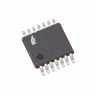
X96012V14I Intersil, X96012V14I Datasheet - Page 12

X96012V14I
Manufacturer Part Number
X96012V14I
Description
IC CNTRLR UNIV MEM/DAC 14-TSSOP
Manufacturer
Intersil
Type
Controllerr
Datasheet
1.X96012V14IZT1.pdf
(23 pages)
Specifications of X96012V14I
Input Type
*
Output Type
*
Interface
2-Wire Serial
Current - Supply
*
Mounting Type
Surface Mount
Package / Case
14-TSSOP
Lead Free Status / RoHS Status
Contains lead / RoHS non-compliant
Available stocks
Company
Part Number
Manufacturer
Quantity
Price
Company:
Part Number:
X96012V14I
Manufacturer:
Intersil
Quantity:
1 050
Part Number:
X96012V14IZ
Manufacturer:
INTERSIL
Quantity:
20 000
Control Register 4
This register is accessed by performing a Read or Write
operation to address 84h of memory. This byte’s volatility is
determined by bit NV1234 in Control register 0.
D2DA7 - D2DA0: D/A 2 DIRECT ACCESS BITS
When bit D2DAS (bit 7 in Control register 5) is set to “1”, the
input to the D/A converter 1 is the content of bits
D2DA-D2DA0, and it is not a row of LUT2. When bit D2DAS
is set to “0” (default) these eight bits are ignored by the
X96012. See Figure 9.
Control Register 5
This register is accessed by performing a Read or Write
operation to address 85h of memory.
I1FSO1 - I1FSO0: CURRENT GENERATOR 1 FULL
SCALE OUTPUT SET BITS (NON-VOLATILE)
These two bits are used to set the full scale output current at
the Current Generator 1 pin, I1. If both bits are set to “0”
(default), an external resistor connected between pin R
V
I1. The other three options are indicated in Table 2. The
direction of this current is set by bit I1DS in Control register
0. See Figure 8.
NOTE: *No external resistor should be connected in these cases
between R
I2FSO1 - I2FSO0: CURRENT GENERATOR 2 FULL
SCALE OUTPUT CURRENT SET BITS (NON-VOLATILE)
These two bits are used to set the full scale output current at
the Current Generator 2 pin, I2. If both bits are set to “0”
(default), an external resistor connected between pin R
Vss, determines the full scale output current available at pin
I2. The other three options are indicated Table 3. The direction
of this current is set by bit I2DS in Control Register 0.
NOTE: *No external resistor should be connected in these cases
between R
SS
I1FSO1
I2FSO1
, determines the full scale output current available at pin
0
0
1
1
0
0
1
1
1
2
and V
and V
I1FSO0
I2FSO2
SS
SS
0
1
0
1
0
1
0
1
.
.
I1 FULL SCALE OUTPUT CURRENT
I2 FULL SCALE OUTPUT CURRENT
TABLE 3.
TABLE 2.
Set externally via pin R
Set externally via pin R2 (Default)
12
±0.85mA*
±0.85mA*
±0.4mA*
±1.3mA*
±0.4mA*
±1.3mA*
1
(Default)
2
1
and
and
X96012
L1DAS: LUT1 DIRECT ACCESS SELECT BIT
(NON-VOLATILE)
When bit L1DAS is set to “0” (default), LUT1 is addressed by
the output of the on-chip A/D converter. When bit L1DAS is
set to “1”, LUT1 is addressed by bits L1DA5 - L1DA0.
D1DAS: D/A 1 DIRECT ACCESS SELECT BIT
(NON-VOLATILE)
When bit D1DAS is set to “0” (default), the input to the D/A
converter 1 is a row of LUT1. When bit D1DAS is set to “1”, that
input is the content of the Control register 3.
L2DAS: LUT2 DIRECT ACCESS SELECT BIT
(NON-VOLATILE)
When bit L2DAS is set to “0” (default), LUT2 is addressed by
the output of the on-chip A/D converter. When bit L2DAS is
set to “1”, LUT2 is addressed by bits L2DA5 - L2DA0.
D2DAS: D/A 2 DIRECT ACCESS SELECT BIT
(NONVOLATILE)
When bit D2DAS is set to “0” (default), the input to the D/A
converter 2 is a row of LUT2. When bit D2DAS is set to “1”, that
input is the content of the Control register 4.
Control Register 6
This register is accessed by performing a Read or Write
operation to address 86h of memory.
WEL: WRITE ENABLE LATCH (VOLATILE)
The WEL bit controls the Write Enable status of the entire
X96012 device. This bit must be set to “1” before any other
Write operation (volatile or nonvolatile). Otherwise, any
proceeding Write operation to memory is aborted and no ACK
is issued after a Data Byte.
The WEL bit is a volatile latch that powers up in the “0” state
(disabled). The WEL bit is enabled by writing 10000000
Control register 6. Once enabled, the WEL bit remains set to “1”
until the X96012 is powered down, and then up again, or until it
is reset to “0” by writing 00000000
A Write operation that modifies the value of the WEL bit will not
cause a change in other bits of Control register 6.
Status Register - ADC Output
This register is accessed by performing a Read operation to
address 87h of memory.
AD7 - AD0: A/D CONVERTER OUTPUT BITS (READ
ONLY)
These eight bits are the binary output of the on-chip A/D
converter. The output is 00000000
11111111
the LUTs.
2
for full scale input. The six MSBs select a row of
2
to Control register 6.
2
for minimum input and
February 20, 2008
2
FN8216.3
to


